A Guide to PCB Assembly Power Supply Layout
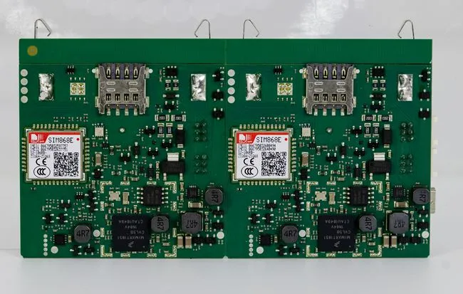
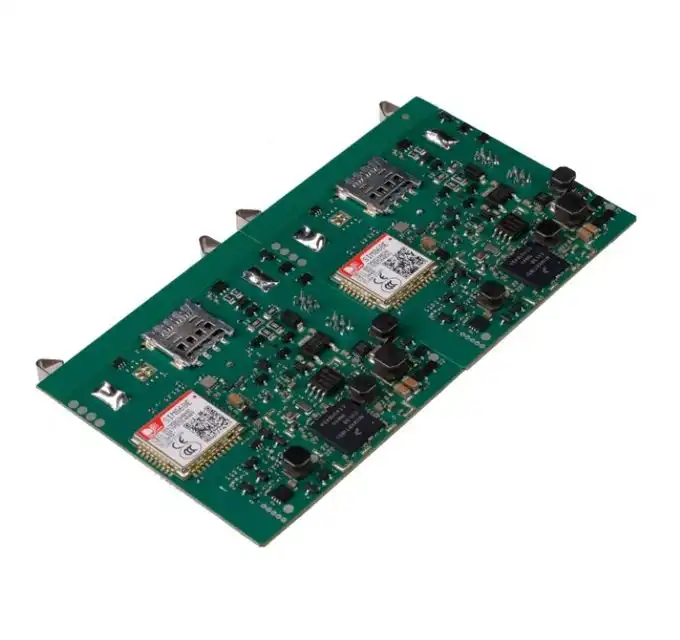
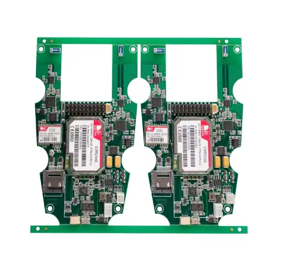
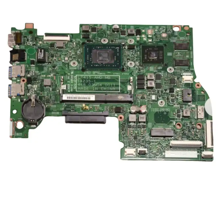
A well-designed PCB assembly power supply layout is crucial for ensuring optimal performance and reliability in electronic devices. This guide explores key considerations for power supply layout in PCB assembly, including component placement, trace routing, and thermal management. By following best practices in power distribution, designers can minimize noise, reduce electromagnetic interference, and enhance overall system efficiency. Proper layout techniques are essential for creating robust power systems that meet the demands of modern electronic applications.

Fundamentals of Power Supply Layout in PCB Assembly
Component Placement Strategies
Effective component placement is the foundation of a successful power supply layout in PCB assembly. Begin by positioning power components, such as voltage regulators and capacitors, close to each other to minimize trace lengths and reduce parasitic inductance. Place high-current components near the power source to minimize voltage drops across the board. Consider grouping components by function, separating analog and digital sections to prevent noise coupling.
When arranging components, pay attention to thermal considerations. Heat-generating components should be placed in areas with good airflow or near heat sinks to facilitate efficient cooling. Avoid placing sensitive components near high-power devices that may cause thermal interference. Additionally, consider the orientation of components to optimize signal flow and minimize crosstalk between adjacent traces.
Power Plane Design Techniques
Implementing proper power plane design is crucial for maintaining stable voltage levels across the PCB. Utilize dedicated power and ground planes to create low-impedance paths for current flow. This approach helps reduce noise and improves overall system performance. When designing power planes, ensure adequate copper thickness to handle the expected current loads without excessive voltage drop or heat generation.
Consider using split power planes for different voltage domains to isolate noise-sensitive circuits. Implement guard traces or keep-out areas around high-frequency signals to prevent interference with power distribution. Pay special attention to the placement of decoupling capacitors, positioning them as close as possible to the power pins of integrated circuits to minimize inductance and provide local charge storage.
Trace Routing Considerations
Proper trace routing is essential for maintaining signal integrity and minimizing electromagnetic interference in PCB assembly power supply layouts. Use wide traces for power distribution to reduce resistance and voltage drop. Calculate the appropriate trace width based on the expected current flow and allowable temperature rise. For high-current paths, consider using multiple layers with vias to increase the effective cross-sectional area of the conductor.
Implement star topology for power distribution, with separate traces branching out from a central power source to individual components. This approach helps minimize voltage variations and reduces the impact of noise on sensitive circuits. Avoid routing high-speed signals parallel to power traces to prevent coupling and maintain signal integrity. Use 45-degree angles for trace corners to reduce reflections and maintain consistent impedance.
Advanced Techniques for Optimizing Power Supply Performance
Decoupling and Bypass Capacitor Placement
Proper placement of decoupling and bypass capacitors is critical for maintaining stable power supply voltages and minimizing noise in PCB assemblies. Position these capacitors as close as possible to the power pins of integrated circuits, using short, wide traces to connect them. Implement a multi-layer decoupling strategy, using a combination of small, medium, and large capacitors to address a wide range of frequencies.
Consider using different capacitor types, such as ceramic and tantalum, to optimize performance across various frequency ranges. Pay attention to the self-resonant frequency of capacitors and select values that provide effective decoupling at the operating frequencies of your circuit. In high-speed designs, use multiple smaller capacitors in parallel rather than a single large capacitor to reduce parasitic inductance and improve high-frequency response.
EMI Reduction Techniques
Implementing effective EMI reduction techniques is crucial for ensuring compliance with regulatory standards and maintaining reliable operation of PCB assemblies. Use ground planes to create low-impedance return paths for currents and minimize loop areas. Implement guard traces around sensitive analog circuits to prevent interference from digital signals. Consider using ferrite beads or common-mode chokes on power lines to attenuate high-frequency noise.
Pay attention to the placement of connectors and I/O interfaces, ensuring proper grounding and shielding to minimize radiated emissions. Implement controlled impedance routing for high-speed signals to reduce reflections and maintain signal integrity. In multi-layer designs, use adjacent power and ground planes to create a low-inductance power distribution network and improve EMI performance.
Thermal Management Strategies
Effective thermal management is essential for maintaining reliable operation and extending the lifespan of PCB assemblies. Implement copper pours and thermal vias to improve heat dissipation from power components. Use multiple layers with interleaved power and ground planes to distribute heat more evenly across the board. Consider using thicker copper for power planes and high-current traces to reduce resistance and minimize heat generation.
Pay attention to component spacing and orientation to allow for proper airflow and prevent hot spots. Implement thermal relief patterns around component pads to balance heat dissipation and solderability. In designs with high-power components, consider using heat sinks or forced-air cooling to maintain acceptable operating temperatures. Use thermal simulation tools during the design phase to identify potential issues and optimize component placement for improved heat dissipation.
Best Practices for Power Supply Layout Verification
Design Rule Checks and Simulations
Implementing rigorous design rule checks (DRCs) and simulations is crucial for verifying the integrity of PCB assembly power supply layouts. Use automated DRC tools to check for violations of spacing, clearance, and trace width requirements. Pay special attention to power-related rules, such as minimum trace widths for high-current paths and thermal relief settings for power pads.
Employ circuit simulation tools to analyze voltage drops, current distribution, and transient response of the power supply network. Use electromagnetic field solvers to identify potential EMI issues and optimize component placement. Perform thermal simulations to verify that components operate within their specified temperature ranges and identify areas that may require additional cooling or heat dissipation measures.
Power Integrity Analysis
Conducting comprehensive power integrity analysis is essential for ensuring stable and reliable operation of PCB assemblies. Use specialized tools to perform DC voltage drop analysis, identifying areas where excessive voltage drop may occur due to trace resistance or insufficient copper. Analyze AC impedance characteristics of the power distribution network to ensure low impedance across the frequency range of interest.
Perform transient analysis to evaluate the power supply's response to sudden load changes and verify that voltage levels remain within acceptable limits. Use advanced techniques such as target impedance analysis to optimize decoupling network performance. Consider implementing on-board voltage and current monitoring to facilitate real-time power integrity verification during operation.
Prototyping and Testing Strategies
Implementing effective prototyping and testing strategies is crucial for validating PCB assembly power supply layouts. Begin with a thorough visual inspection of the assembled board, checking for proper component placement, solder quality, and overall workmanship. Use thermal imaging cameras to identify hot spots and verify that thermal management measures are effective.
Perform comprehensive electrical testing, including voltage and current measurements at key points in the power distribution network. Use oscilloscopes and spectrum analyzers to evaluate noise levels and identify any unexpected high-frequency components. Conduct EMI testing to ensure compliance with relevant standards and verify the effectiveness of implemented noise reduction techniques. Consider environmental testing, such as temperature cycling and vibration analysis, to evaluate the robustness of the power supply layout under various operating conditions.
Conclusion
Mastering PCB assembly power supply layout is crucial for creating reliable and high-performance electronic devices. By implementing proper component placement, power plane design, and trace routing techniques, designers can optimize power distribution and minimize noise in their circuits. Advanced strategies such as effective decoupling, EMI reduction, and thermal management further enhance the performance and reliability of PCB assemblies.
Optimized Power Layout for Enhanced Thermal and Signal Integrity | Ring PCB
Ring PCB Technology Co., Limited offers comprehensive one-stop PCB and PCBA services, ensuring reliability at every stage. With 17 years of excellence, we specialize in innovative solutions for diverse industries. Our advanced engineering capabilities include high-density stack-ups, precision manufacturing, and adherence to stringent quality standards. Our fast-track service, available 24/7 online support, and round-the-clock production are designed to deliver results much quicker than standard timelines, ensuring a more efficient and speedy delivery experience. For expert guidance on optimizing your PCB assembly power supply layout, contact us at [email protected].
References
1. Johnson, H. W., & Graham, M. (2003). High-speed digital design: a handbook of black magic. Prentice Hall PTR.
2. Ott, H. W. (2011). Electromagnetic compatibility engineering. John Wiley & Sons.
3. Bogatin, E. (2018). Signal and power integrity-simplified. Prentice Hall Press.
4. Wang, P. (2016). Thermal management of electronic systems: From component to system. Springer.
5. Montrose, M. I. (2004). EMC and the printed circuit board: design, theory, and layout made simple. John Wiley & Sons.

Welcome to Ring PCB! Share your inquiry, and receive a tailored quotation!

Ring PCB, your trusted partner for PCB & PCBA Full Turnkey Solutions


