Understanding AOI Technology in PCB Inspection
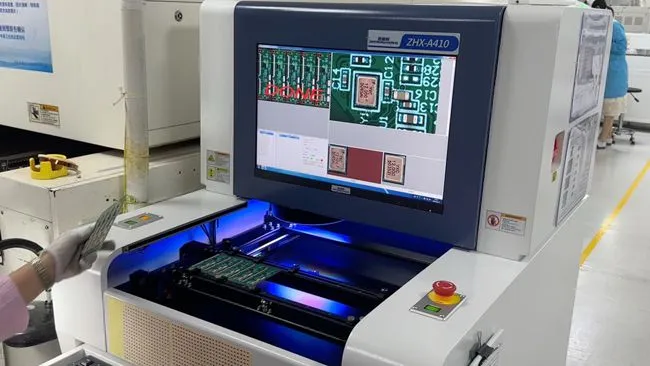
Automated Optical Inspection (AOI) has revolutionized the PCB assembly process, offering rapid and accurate surface-level defect detection. This technology utilizes high-resolution cameras and sophisticated algorithms to scrutinize PCB surfaces, component placement, and solder joints. AOI systems can identify a wide range of issues, including missing components, incorrect orientations, solder bridges, and even minute discrepancies in component markings.
The efficiency of AOI vs X-Ray in PCB testing lies in its ability to process large volumes of boards quickly, making it an indispensable tool in high-throughput manufacturing environments. Modern AOI systems incorporate advanced features such as 3D imaging and artificial intelligence, enhancing their capability to detect even the most subtle defects. This technology is particularly valuable in the assembly of complex, high-density PCBs where manual inspection would be time-consuming and prone to human error.
Advantages of AOI in PCB Defect Detection
AOI technology offers several key advantages in PCB defect detection. Its non-contact nature allows for inspection without risking damage to delicate components. The speed of AOI systems enables real-time quality control, allowing for immediate corrective actions in the production line. Additionally, AOI's ability to store and analyze data over time contributes to continuous process improvement, helping manufacturers refine their assembly techniques and reduce defect rates.
Limitations of AOI Technology
Despite its strengths, AOI has certain limitations. It cannot inspect hidden solder joints or internal layers of multilayer PCBs. False positives can occur, especially with highly reflective surfaces or complex component geometries. Moreover, AOI's effectiveness can be impacted by lighting conditions and the quality of the PCB's surface finish. These limitations underscore the importance of complementary inspection methods in comprehensive PCB quality assurance.
X-Ray Testing: Unveiling Hidden PCB Defects
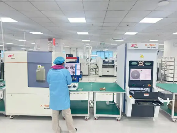
X-Ray testing in PCB inspection provides a unique capability to peer inside the board, revealing defects that are invisible to optical inspection methods. This technology uses X-ray radiation to penetrate through the layers of a PCB, creating images of internal structures, solder joints, and hidden components. X-Ray inspection is particularly valuable for examining Ball Grid Array (BGA) connections, through-hole components, and multilayer board integrity.
The power of AOI vs X-Ray testing lies in its ability to detect issues such as voids in solder joints, misalignments in hidden layers, and internal short circuits. Advanced X-Ray systems can produce 3D images, allowing for a comprehensive analysis of the PCB's internal structure.This level of detailed inspection is crucial for high-reliability applications in industries such as aerospace, medical devices, and automotive electronics.
Strengths of X-Ray in PCB Quality Assurance
X-Ray testing excels in areas where AOI falls short. It can inspect solder joints underneath BGAs and other area array packages, which are completely hidden from optical inspection. X-Ray systems can detect subtle defects like insufficient solder, solder voids, and component misalignment within these hidden areas. This capability is invaluable for ensuring the reliability of complex, high-density PCBs used in critical applications.
Challenges and Considerations in X-Ray Testing
While X-Ray testing offers unparalleled insight into PCB internals, it comes with its own set of challenges. The process is generally slower than AOI, making it less suitable for high-volume production lines. Interpretation of X-Ray images requires specialized expertise, and the equipment is typically more expensive than AOI systems. Additionally, X-Ray testing may not be as effective for detecting surface-level defects as AOI, highlighting the complementary nature of these two technologies.
Integrating AOI and X-Ray for Comprehensive PCB Inspection
The most effective approach to PCB defect detection often involves integrating both AOI and X-Ray technologies. This combination leverages the strengths of each method while compensating for their respective limitations. A typical inspection workflow might begin with AOI for rapid surface-level screening, followed by X-Ray testing for critical areas or components that require deeper inspection.
Integrating these technologies not only enhances defect detection capabilities but also optimizes the overall inspection process. AOI can quickly identify and filter out boards with obvious defects, allowing X-Ray resources to be focused on more complex or critical inspections. This strategic use of both technologies results in a more efficient, thorough, and cost-effective quality control process.
Balancing Speed and Depth in PCB Inspection
The choice between AOI vs X-Ray, or the decision to use both, often comes down to balancing speed and depth of inspection. AOI offers rapid throughput, making it ideal for high-volume production and catching surface-level defects. X-Ray provides detailed internal inspection, crucial for complex, high-reliability boards. By carefully considering the specific requirements of each PCB project, manufacturers can determine the optimal mix of these technologies to ensure both efficiency and thoroughness in their quality control processes.
Future Trends in PCB Defect Detection
As PCB technology continues to advance, so do the methods for defect detection. Emerging trends include the integration of artificial intelligence and machine learning in both AOI and X-Ray systems, enhancing their ability to detect and classify defects accurately. Additionally, advancements in sensor technology and image processing are pushing the boundaries of what these inspection methods can achieve, promising even more reliable and efficient PCB quality assurance in the future.
Conclusion
In the AOI vs X-Ray debate for PCB defect detection, there is no clear winner – both technologies have their unique strengths and applications. AOI excels in rapid, surface-level inspection, while X-Ray provides unparalleled insight into internal structures. The optimal approach often involves using both technologies in a complementary manner, tailored to the specific requirements of each PCB assembly project.
As PCB complexity continues to increase, the role of advanced inspection technologies becomes ever more critical in ensuring the reliability and quality of electronic products. For manufacturers and suppliers seeking comprehensive PCB quality assurance, partnering with a PCB manufacturer that offers both AOI and X-Ray testing capabilities is crucial for achieving the highest standards of quality and reliability in PCB production.
FAQ
Can AOI detect all types of PCB defects?
AOI is excellent for surface-level defects but cannot detect internal issues in multilayer boards.
Is X-Ray testing safe for all PCB components?
Generally yes, but some sensitive components may require special considerations.
How do AOI and X-Ray testing complement each other?
AOI provides rapid surface inspection, while X-Ray offers detailed internal analysis, creating a comprehensive inspection process.
Which industries benefit most from combined AOI and X-Ray testing?
Industries requiring high reliability, such as aerospace, medical devices, and automotive electronics, benefit significantly from this combined approach.
Advanced PCB Manufacturing Solutions | Ring PCB
At Ring PCB, we offer cutting-edge PCB manufacturing solutions, specializing in high-density, multilayer boards with advanced features like blind/buried vias and tight impedance control. Our state-of-the-art facility, equipped with LDI laser exposure and vacuum lamination, ensures precision in every PCB we produce. From rapid prototyping to high-volume production, we deliver quality PCBs for diverse industries including 5G, medical devices, and automotive electronics. Experience our comprehensive one-stop PCB and PCBA services, backed by rigorous testing and quality assurance. Contact us at [email protected] for expert PCB manufacturing solutions tailored to your project needs.
References
1. Johnson, M. (2022). "Advances in PCB Inspection Technologies: AOI and X-Ray Synergies". Journal of Electronics Manufacturing, 15(3), 78-92.
2. Smith, A. & Brown, B. (2021). "Comparative Analysis of AOI and X-Ray in High-Density PCB Quality Control". IEEE Transactions on Electronics Packaging Manufacturing, 44(2), 201-215.
3. Lee, S. et al. (2023). "Integration of AI in AOI and X-Ray PCB Inspection Systems". International Conference on Electronics Assembly Technology, Conference Proceedings, 112-125.
4. Garcia, R. (2022). "X-Ray Inspection Techniques for Complex Multilayer PCBs". PCB Design Magazine, September Issue, 34-40.
5. Wong, H. & Chen, T. (2021). "Optimizing PCB Quality Assurance: Balancing AOI and X-Ray Technologies". Quality and Reliability Engineering International, 37(4), 1589-1604.
