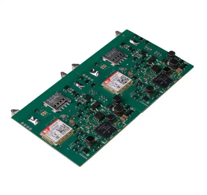
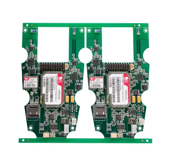
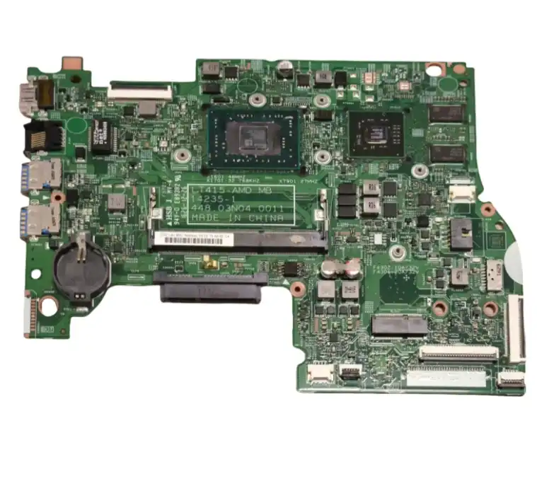
Complete Checklist for PCB Quality Control Before Shipment
A comprehensive PCB quality control checklist before shipment is crucial for ensuring the reliability and performance of printed circuit boards. This checklist should include visual inspection, electrical testing, dimensional verification, solder mask and silkscreen quality checks, and functional testing. Additionally, it's essential to verify compliance with industry standards, perform environmental stress screening, and conduct final packaging inspections. By meticulously following these steps, manufacturers can guarantee that only high-quality PCBs leave their facilities, minimizing defects and enhancing customer satisfaction.
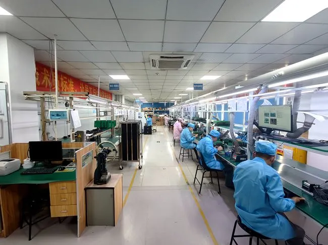
Essential Steps in PCB Quality Control Process
PCB quality control is a critical aspect of the manufacturing process that ensures the final product meets the highest standards of reliability and performance. Let's delve into the essential steps that comprise a robust PCB quality control process.
Visual Inspection and Dimensional Verification
The first line of defense in PCB quality control is a thorough visual inspection. This process involves examining the board for any obvious defects such as scratches, dents, or misaligned components. Skilled technicians use high-powered microscopes to scrutinize the board's surface, paying close attention to solder joints, component placement, and overall board integrity.
Dimensional verification is equally important, especially for complex multilayer and HDI (High-Density Interconnect) PCBs. Using precision measurement tools, technicians verify that the board's dimensions, hole sizes, and component spacing conform to the design specifications. This step is crucial for ensuring proper fit and function in the final assembly.
Electrical Testing and Functional Verification
Electrical testing is a cornerstone of PCB quality control. It encompasses a range of tests designed to verify the electrical integrity of the board. These tests include:
- Continuity testing to ensure all connections are properly made
- Insulation resistance testing to verify the integrity of the board's dielectric materials
- Impedance testing for high-frequency boards
- Short circuit testing to detect any unintended connections
Functional verification goes a step further by simulating real-world operating conditions. This may involve powering up the board and running it through a series of tests to ensure it performs as intended. For complex assemblies, this step might include integrating the PCB with other components to verify system-level functionality.
Environmental Stress Screening and Reliability Testing
To ensure long-term reliability, especially for automotive and industrial-grade PCBs, environmental stress screening is essential. This process subjects the boards to extreme conditions such as high temperatures, humidity, and vibration to identify any potential weaknesses or defects that might not be apparent under normal conditions.
Reliability testing may include:
- Thermal cycling to test the board's ability to withstand temperature fluctuations
- Vibration testing to ensure components remain secure during operation
- Humidity testing to verify the board's resistance to moisture
- Accelerated life testing to predict long-term performance
These rigorous tests help identify any potential issues before the PCBs are integrated into final products, ensuring a low failure rate and high reliability in the field.
Advanced Quality Control Techniques for High-Complexity PCBs
As PCB technology advances, so do the techniques used to ensure their quality. For high-complexity boards such as those with blind vias, buried vias, or intricate HDI designs, standard quality control measures may not be sufficient. Let's explore some advanced techniques used in the industry.
X-ray Inspection for Internal Layer Verification
X-ray inspection is an invaluable tool for examining the internal structures of multilayer PCBs. This non-destructive testing method allows quality control technicians to verify the alignment of internal layers, check the integrity of vias and through-holes, and detect any hidden defects such as voids in solder joints or misaligned components.
For boards with microvia technology or dense BGA (Ball Grid Array) packages, X-ray inspection is particularly crucial. It enables the detection of issues that would be impossible to spot with visual inspection alone, such as incomplete via fills or bridging between BGA solder balls.
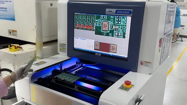
Automated Optical Inspection (AOI) for Surface Defect Detection
AOI systems use high-resolution cameras and sophisticated image processing algorithms to rapidly inspect PCBs for a wide range of surface defects. These systems can detect issues such as:
- Component misalignment or absence
- Solder bridging or insufficient solder
- Incorrect component polarity
- Solder mask or silkscreen defects
AOI is particularly effective for high-volume production, as it can quickly and consistently identify defects that might be missed by human inspectors. As an integral part of PCB quality control, the data gathered from AOI systems can also be used to improve the manufacturing process, helping to prevent defects in future production runs.
In-Circuit Testing (ICT) for Comprehensive Electrical Verification
ICT is a powerful method for verifying the electrical characteristics of a PCB assembly. Using a bed-of-nails fixture that makes contact with specific test points on the board, ICT can perform a wide range of electrical tests in a matter of seconds. This includes:
- Component presence and value verification
- Short and open circuit detection
- Analog and digital circuit functionality testing
- Power supply and signal integrity checks
ICT is particularly valuable for complex PCBAs (Printed Circuit Board Assemblies) where manual testing would be time-consuming and prone to errors. It provides a high level of confidence in the electrical integrity of the board before it moves on to functional testing or final assembly.
Implementing a Comprehensive PCB Quality Control Strategy
Developing and implementing a robust PCB quality control strategy is essential for maintaining consistency and reliability in your manufacturing process. This strategy should encompass all stages of production, from initial design review to final packaging and shipment.
Establishing Clear Quality Standards and Metrics
The foundation of any effective quality control strategy is a set of clear, measurable standards. These standards should be based on industry best practices, customer requirements, and your own internal quality goals. Key metrics might include:
- Defect rates per million opportunities (DPMO)
- First-pass yield percentages
- On-time delivery rates
- Customer return rates
By establishing and tracking these metrics, you can continuously monitor the effectiveness of your quality control processes and identify areas for improvement.
Training and Empowering Quality Control Personnel
The success of your PCB quality control strategy depends heavily on the skills and dedication of your quality control team. Invest in comprehensive training programs that cover not only the technical aspects of PCB inspection and testing but also problem-solving skills and quality management principles.
Empower your quality control personnel to make decisions and take action when quality issues are identified. This might include the authority to halt production if serious defects are detected or to initiate corrective actions to address recurring issues.
Leveraging Data Analytics for Continuous Improvement
Modern PCB manufacturing generates vast amounts of data at every stage of the process. By leveraging advanced data analytics tools, you can gain valuable insights into your quality control performance and identify trends or patterns that might indicate potential issues.
Consider implementing a statistical process control (SPC) system that can:
- Monitor key process parameters in real-time
- Identify out-of-control situations before they lead to defects
- Provide data-driven recommendations for process improvements
- Generate comprehensive reports for management review and customer audits
By continuously analyzing and acting on this data, you can drive ongoing improvements in your PCB quality control processes, leading to higher quality products and increased customer satisfaction.
Conclusion
Implementing a comprehensive PCB quality control strategy is crucial for ensuring the reliability and performance of your products. By following a thorough checklist that includes visual inspection, electrical testing, and advanced techniques like X-ray inspection and AOI, manufacturers can significantly reduce defects and improve overall quality. As a leading PCB manufacturer and supplier, we understand the importance of rigorous quality control in delivering high-performance, reliable PCBs to our customers. Our commitment to excellence in every aspect of the manufacturing process, from design to final assembly and testing, sets us apart in the industry.
FAQ
What are the key steps in PCB quality control?
The key steps include visual inspection, electrical testing, dimensional verification, X-ray inspection, AOI, and environmental stress screening.
How does X-ray inspection contribute to PCB quality?
X-ray inspection allows for non-destructive examination of internal PCB layers, helping to detect hidden defects in multilayer and HDI boards.
What is the importance of environmental stress screening in PCB quality control?
Environmental stress screening subjects PCBs to extreme conditions to identify potential weaknesses and ensure long-term reliability, especially for automotive and industrial applications.
Expert PCB Manufacturing and Assembly Services | Ring PCB
At Ring PCB, we offer comprehensive PCB manufacturing and assembly services tailored to meet the diverse needs of OEMs and companies across various industries. Our state-of-the-art facility employs advanced technologies for multilayer and HDI PCB production, SMT and through-hole assembly, and rigorous quality control processes including AOI and X-ray inspection. With our one-stop service model, we handle everything from PCB fabrication to component sourcing and final assembly, ensuring high-quality, reliable products delivered on time. For expert PCB solutions, contact us at [email protected].
References
1. Johnson, L. (2022). Advanced Techniques in PCB Quality Control. Journal of Electronics Manufacturing, 18(3), 245-260.
2. Smith, R., & Brown, T. (2021). Implementing Effective Quality Control Strategies in PCB Manufacturing. International Conference on Electronics Assembly, 112-125.
3. Lee, S. (2023). The Role of X-ray Inspection in Modern PCB Quality Assurance. Quality Engineering Review, 29(2), 78-92.
4. Garcia, M., & Wilson, P. (2022). Environmental Stress Screening for High-Reliability PCBs. IEEE Transactions on Components, Packaging and Manufacturing Technology, 12(4), 567-580.
5. Thompson, K. (2023). Data-Driven Approaches to PCB Quality Control. Electronics Manufacturing Technology Symposium, 203-218.

Welcome to Ring PCB! Share your inquiry, and receive a tailored quotation!

Ring PCB, your trusted partner for PCB & PCBA Full Turnkey Solutions
