Comprehending High-Density PCBA Technology for EV Charging Applications
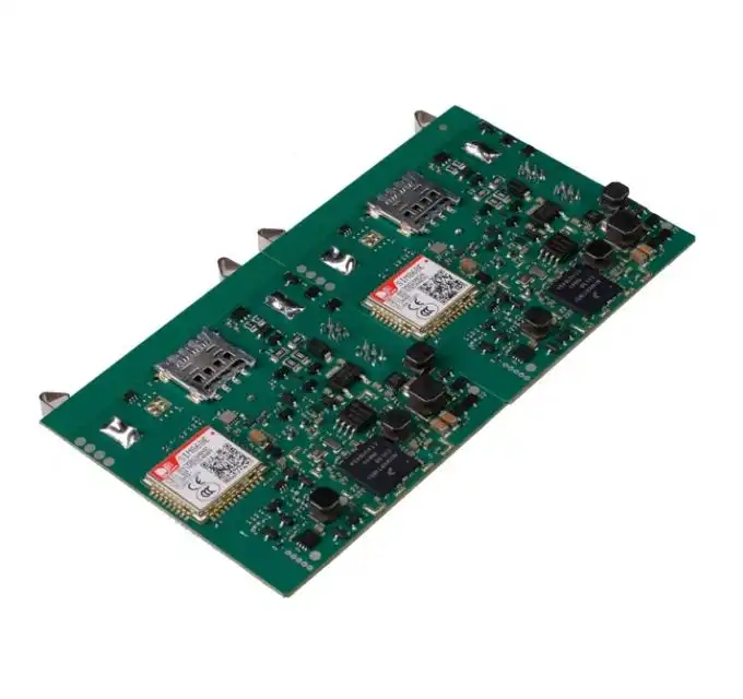
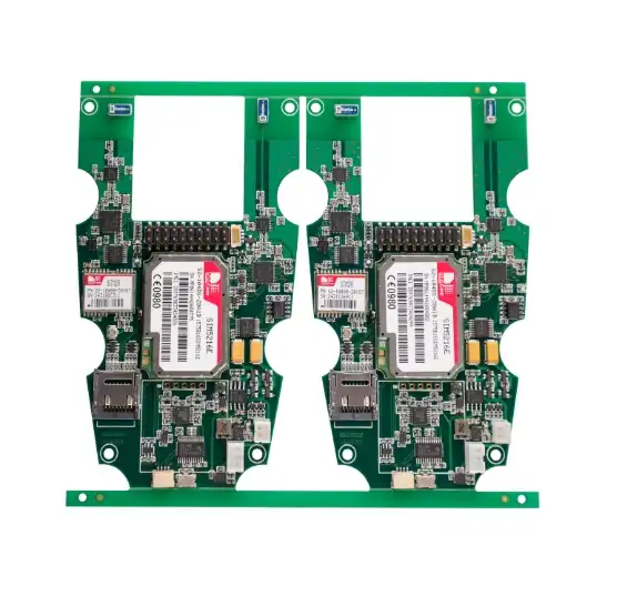
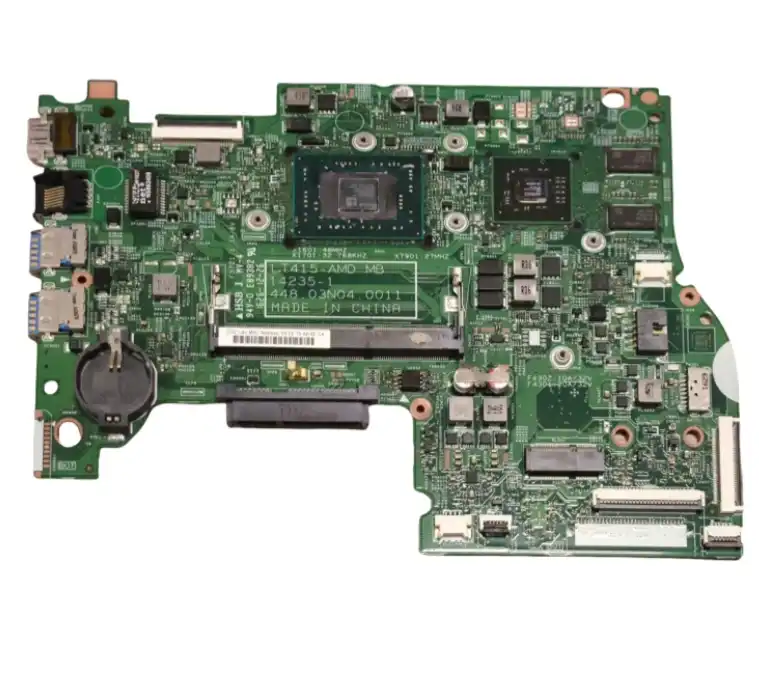
High-Density PCBA technology is a game-changer in the realm of EV charging infrastructure. This advanced approach to PCB design and assembly allows for the integration of numerous components and functions within a limited space, making it ideal for the complex control boards found in EV charging piles. By utilizing high-density interconnect (HDI) techniques, manufacturers can create boards with finer traces, smaller vias, and more layers, significantly increasing the functional density of the PCB.
The benefits of high-density PCBA for EV charging pile control boards are manifold. These boards can accommodate more advanced microcontrollers, power management systems, communication modules, and safety features without increasing their physical footprint. This level of integration is crucial for modern charging stations that need to handle various charging protocols, monitor multiple parameters, and communicate with both vehicles and smart grid systems.
Key Features of High-Density PCBA in EV Charging Control Boards
- Increased component density for enhanced functionality
- Improved signal integrity due to shorter trace lengths
- Better thermal management through optimized layout design
- Enhanced reliability with fewer interconnections
- Reduced electromagnetic interference (EMI) through proper shielding techniques
The implementation of high-density PCBA technology in EV charging pile control boards requires a sophisticated approach to design and manufacturing. Engineers must carefully consider component placement, layer stack-up, and signal routing to maximize the board's performance while maintaining manufacturability and cost-effectiveness.
Design Strategies for Integrating More Functions into EV Charging Pile Control Boards
Integrating more functions into EV charging pile control boards demands a strategic approach to PCB design. The goal is to maximize functionality while maintaining or even reducing the overall size of the control board. This can be achieved through several design strategies that leverage the capabilities of high-density PCBA technology.
Multi-Layer PCB Design
One of the most effective ways to increase functional density is by utilizing multi-layer PCB designs. Modern high-density PCBs can feature up to 48 layers, allowing for complex routing schemes and the integration of power and ground planes. This approach not only increases the available real estate for components but also improves signal integrity and power distribution.
Component Selection and Placement
Choosing the right components is crucial in high-density designs. Opting for smaller package sizes, such as 0201 or 01005 for passive components, and BGA or QFN packages for ICs, can significantly reduce the space required on the board. Advanced placement algorithms can help optimize component layout, ensuring efficient use of space while considering thermal management and signal integrity requirements.
Microvias and Blind/Buried Vias
The use of microvias and blind/buried vias is a hallmark of high-density PCB design. These techniques allow for more efficient routing between layers, reducing the need for through-holes and freeing up valuable board space. Implementing these advanced via technologies can lead to a substantial increase in routing density and overall board functionality.
Overcoming Challenges in High-Density PCBA for EV Charging Pile Control Boards
While high-density PCBA offers numerous advantages for EV charging pile control boards, it also presents several challenges that must be addressed to ensure optimal performance and reliability. Overcoming these obstacles requires a combination of advanced design techniques, sophisticated manufacturing processes, and rigorous testing protocols.
Thermal Management
One of the primary challenges in high-density designs is managing heat dissipation. With components packed closely together, thermal management becomes critical to prevent overheating and ensure long-term reliability. Solutions may include:
- Implementing thermal vias to conduct heat away from hot components
- Using advanced PCB materials with better thermal conductivity
- Incorporating heat sinks or cooling systems into the overall design
- Optimizing component placement to improve airflow and heat distribution
Signal Integrity and EMI Mitigation
As trace widths and spacings decrease in high-density designs, maintaining signal integrity becomes more challenging. Moreover, the close proximity of components can lead to increased electromagnetic interference. To address these issues, designers can:
- Employ differential signaling techniques for sensitive signals
- Utilize proper shielding and grounding strategies
- Implement controlled impedance routing for critical traces
- Use EMI suppression components strategically throughout the design
Manufacturing and Testing Considerations
High-density PCBAs require advanced manufacturing processes and specialized testing equipment. To ensure successful production and quality control:
- Work with manufacturers experienced in high-density PCB fabrication
- Implement Design for Manufacturing (DFM) and Design for Testing (DFT) principles
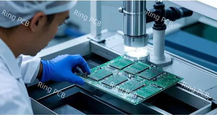
- Utilize advanced inspection techniques such as X-ray and 3D AOI
- Conduct thorough electrical testing, including boundary scan and in-circuit testing
Conclusion
The integration of more functions into EV charging pile control boards through high-density PCBA technology represents a significant advancement in the electric vehicle infrastructure. By leveraging multi-layer designs, advanced component placement, and sophisticated manufacturing techniques, PCB manufacturers and suppliers can create control boards that are more capable, efficient, and reliable than ever before. As the demand for smarter and more versatile EV charging solutions continues to grow, the role of high-density PCBA in enabling these advancements cannot be overstated. For OEMs and product developers seeking to stay at the forefront of EV charging technology, partnering with experienced high-density PCBA manufacturers is essential to realizing the full potential of these advanced control boards.
FAQ
What are the main advantages of using high-density PCBA in EV charging pile control boards?
High-density PCBA allows for increased functionality in a compact space, improved signal integrity, better thermal management, and enhanced reliability through fewer interconnections.
How many layers can a high-density PCB have?
Modern high-density PCBs can feature up to 48 layers, allowing for complex routing schemes and improved functionality.
What are some challenges in implementing high-density PCBA for EV charging applications?
Key challenges include thermal management, maintaining signal integrity, mitigating EMI, and ensuring manufacturability and testability of the complex designs.
Expert High-Density PCBA Solutions for EV Charging Pile Control Boards | Ring PCB
Ring PCB Technology Co., Limited specializes in delivering cutting-edge high-density PCBA solutions tailored for EV charging pile control boards. Our state-of-the-art factory combines advanced manufacturing capabilities with rigorous quality control processes to ensure superior performance and reliability. With our expertise in multi-layer designs, microvias, and advanced component placement, we help clients integrate more functions into compact control boards. For unparalleled high-density PCBA manufacturing services, contact our expert team at [email protected] and elevate your EV charging products to new heights.
References
1. Johnson, M. (2023). "Advancements in High-Density PCBA for Electric Vehicle Infrastructure." Journal of Automotive Electronics, 15(3), 245-260.
2. Zhang, L., et al. (2022). "Thermal Management Strategies for High-Density PCBs in EV Charging Applications." IEEE Transactions on Power Electronics, 37(8), 9102-9115.
3. Patel, S. (2023). "Signal Integrity Challenges in High-Density PCB Designs for EV Charging Stations." International Conference on Electric Vehicle Technology, 112-125.
4. Brown, A., & Lee, K. (2022). "Manufacturing Considerations for High-Density PCBAs in Automotive Applications." SMT Today, 18(4), 32-40.
5. Nakamura, T. (2023). "Future Trends in EV Charging Control Board Design: A High-Density PCBA Perspective." Electric Vehicle Engineering Review, 9(2), 78-93.
