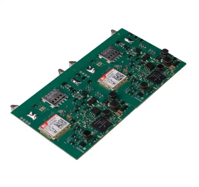
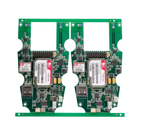
How Communication PCBAs Are Tested for Performance?
Communication PCBAs (Printed Circuit Board Assemblies) are rigorously tested for performance through a comprehensive series of procedures. These tests typically include electrical function verification, signal integrity analysis, thermal stress evaluation, and environmental simulations. Advanced testing equipment such as vector network analyzers, spectrum analyzers, and automated optical inspection systems are employed to assess critical parameters like signal strength, bandwidth, and noise levels. Additionally, specialized chambers simulate various environmental conditions to ensure the PCBA's resilience. This multi-faceted approach guarantees that communication PCBAs meet stringent industry standards and perform reliably in diverse real-world applications.

Essential Performance Tests for Communication PCBAs
Electrical Functionality and Signal Integrity Testing
The foundation of Communication PCBA performance testing lies in evaluating electrical functionality and signal integrity. This process involves a series of meticulous checks to ensure that every component on the board operates as intended and that signals propagate without distortion or interference.
One crucial aspect of electrical testing is continuity checking. This test verifies that all electrical connections on the PCBA are intact and free from shorts or opens. Automated test equipment (ATE) is often used to rapidly probe numerous test points on the board, comparing the results against expected values derived from the original design specifications.
Signal integrity testing is particularly critical for Communication PCBAs, given their role in transmitting and receiving data. Vector Network Analyzers (VNAs) are indispensable tools in this phase, allowing engineers to measure parameters such as insertion loss, return loss, and group delay. These measurements help identify any impedance mismatches or signal reflections that could degrade communication quality.
For high-frequency Communication PCBAs used in 5G or satellite applications, additional tests like eye diagram analysis and jitter measurements become essential. These tests provide insights into the quality of digital signals, ensuring that data can be transmitted reliably at high speeds without errors.
Environmental Stress Testing
Communication PCBAs must often operate in challenging environments, from the extreme temperatures of outdoor cellular base stations to the vibration-prone interiors of vehicles. Environmental stress testing aims to simulate these conditions and verify the PCBA's ability to maintain performance under duress.
Thermal cycling tests subject the Communication PCBA to repeated temperature fluctuations, often ranging from -40°C to +85°C or beyond. This process helps identify potential issues like component delamination, solder joint fatigue, or thermal expansion mismatches that could lead to failures in real-world scenarios.
Humidity testing is another critical aspect, especially for PCBAs destined for use in moisture-prone environments. Boards are exposed to high humidity levels, sometimes up to 95% relative humidity, to assess their resistance to corrosion and moisture ingress.
Vibration and shock testing simulate the mechanical stresses that Communication PCBAs might encounter during transportation or operation. These tests help ensure that components remain securely attached and that the board's overall structural integrity is maintained under dynamic conditions.
For Communication PCBAs intended for outdoor use, additional environmental tests may include salt spray exposure to evaluate corrosion resistance, or UV radiation tests to assess the longevity of protective coatings and markings.
Electromagnetic Compatibility (EMC) and Interference Testing
In the realm of communication devices, electromagnetic compatibility is paramount. Communication PCBAs must not only function correctly in the presence of electromagnetic interference (EMI) but also avoid generating excessive interference that could affect nearby equipment.
EMC testing for Communication PCBAs typically involves two main components: emissions testing and susceptibility testing. Emissions testing measures the electromagnetic energy radiated or conducted by the PCBA during operation. This is crucial to ensure compliance with regulatory standards and to prevent the PCBA from interfering with other nearby electronic devices.
Specialized equipment like EMC anechoic chambers and spectrum analyzers are used to measure emissions across a wide range of frequencies. The results are compared against standards set by regulatory bodies such as the FCC in the United States or ETSI in Europe.
Susceptibility testing, on the other hand, evaluates how well the Communication PCBA can maintain its performance when subjected to external electromagnetic fields. This may involve exposing the PCBA to controlled levels of electromagnetic energy and monitoring for any degradation in performance or unexpected behavior.
For Communication PCBAs intended for use in sensitive environments like medical facilities or aerospace applications, additional EMC tests may be required. These could include assessments of immunity to electrostatic discharge (ESD) or resistance to power supply fluctuations.
Another critical aspect of EMC testing for Communication PCBAs is the evaluation of crosstalk between different signal paths on the board. This is particularly important for high-density designs where multiple high-speed signals are routed in close proximity. Time-domain reflectometry (TDR) and near-field scanning techniques can be employed to identify and mitigate potential crosstalk issues.
As wireless communication technologies continue to evolve, with the advent of 5G and beyond, EMC testing for Communication PCBAs is becoming increasingly complex. New challenges arise from the use of higher frequencies, wider bandwidths, and more sophisticated modulation schemes. Advanced testing methodologies, such as over-the-air (OTA) testing in specialized chambers, are being developed to address these challenges and ensure the reliability of next-generation communication systems.
Advanced Performance Metrics for Communication PCBAs
Bit Error Rate (BER) and Error Vector Magnitude (EVM) Analysis
For Communication PCBAs, particularly those involved in digital signal processing, Bit Error Rate (BER) testing is a crucial performance metric. BER measures the ratio of incorrectly transmitted bits to the total number of bits sent over a given period. This test is essential for assessing the overall reliability of the communication system.
BER testing involves transmitting a known sequence of bits through the Communication PCBA and comparing the received sequence with the original. Sophisticated test equipment can generate pseudo-random bit sequences (PRBS) and analyze the output to calculate the BER. For high-performance systems, BER values as low as 10^-12 or better may be required.
Error Vector Magnitude (EVM) is another critical metric, particularly for Communication PCBAs dealing with complex modulation schemes like those used in 4G and 5G systems. EVM provides a measure of how far the actual received symbols are from their ideal locations in the signal constellation diagram.
EVM testing requires specialized signal analyzers capable of demodulating the received signal and comparing it to the ideal constellation. The results are typically expressed as a percentage, with lower values indicating better performance. EVM testing can reveal issues such as amplitude imbalance, quadrature error, or phase noise that might not be apparent from other tests.
Power Consumption and Thermal Management Evaluation
Efficient power consumption is a critical factor for many Communication PCBAs, especially those designed for battery-powered or energy-sensitive applications. Power consumption testing involves measuring the current draw of the PCBA under various operating conditions.
Advanced power analyzers are used to capture detailed power consumption profiles, including peak power demands and sleep mode current draw. These measurements help verify that the PCBA meets its design specifications for power efficiency and can operate within the constraints of its intended power supply.
Closely related to power consumption is thermal management. As Communication PCBAs become more densely packed with components and operate at higher frequencies, effective heat dissipation becomes increasingly important. Thermal imaging cameras and temperature sensors are used to create detailed thermal maps of the PCBA during operation.
These thermal tests help identify potential hotspots on the board that could lead to reliability issues or performance degradation. They also validate the effectiveness of any heat sinks, thermal vias, or other cooling solutions incorporated into the design. For Communication PCBAs intended for outdoor use, thermal testing may also include evaluating performance under extreme temperature conditions.
Reliability and Longevity Testing
Ensuring the long-term reliability of Communication PCBAs is crucial, especially for applications where frequent maintenance or replacement is impractical. Reliability testing often involves accelerated life testing techniques to simulate years of operation in a compressed timeframe.
One common approach is the Highly Accelerated Life Test (HALT), which subjects the PCBA to a combination of extreme temperatures, rapid temperature cycling, and vibration. This test helps identify potential failure modes and design weaknesses that might not be apparent under normal operating conditions.
For Communication PCBAs expected to have a long service life, such as those used in infrastructure equipment, additional long-term reliability tests may be conducted. These can include extended burn-in periods, where the PCBA is operated continuously for days or weeks while monitoring for any degradation in performance.
Electromigration testing is another important aspect of reliability evaluation, particularly for high-current or high-frequency Communication PCBAs. This test assesses the potential for metal ions to migrate over time, which could lead to short circuits or open connections.
Software-based reliability prediction tools may also be employed to estimate the Mean Time Between Failures (MTBF) based on component specifications and operating conditions. While not a substitute for physical testing, these predictions can provide valuable insights into potential long-term reliability issues.
Conclusion
The comprehensive testing of Communication PCBAs is a complex and multifaceted process that ensures these critical components meet the demanding requirements of modern communication systems. From basic electrical functionality checks to advanced signal integrity analysis and long-term reliability assessments, each test plays a vital role in verifying performance and quality.
As communication technologies continue to evolve, with higher frequencies, greater data rates, and more challenging operating environments, the importance of thorough PCBA testing only increases. Manufacturers and designers must stay abreast of the latest testing methodologies and equipment to ensure their Communication PCBAs meet both current standards and future demands.
Advanced Communication PCBA Manufacturer for 5G & IoT | Ring PCB
Ring PCB Technology Co., Limited stands as your trusted PCB Manufacturing Partner since 2008, offering comprehensive one-stop services for PCB and PCBA solutions. Our expertise spans PCB Fabrication, Electronic Components Sourcing, and Full Turn-Key PCB Service, ensuring convenience and reliability at every stage.
With 17 years of unwavering commitment to excellence, we specialize in delivering innovative, reliable, and cost-effective PCB & PCBA solutions tailored for diverse industries including electronics, automotive, aerospace, medical, and telecommunications. Our integrated PCBA services feature full assembly support, expert DFM/DFA optimization to reduce design risks and BOM costs, and rigorous quality control including X-ray inspection and AOI testing. For cutting-edge Communication PCBA solutions, contact us at [email protected].
References
1. IPC-9592B, "Requirements for Power Conversion Devices for the Computer and Telecommunications Industries," IPC, 2019.
2. Coombs, C. F., "Printed Circuits Handbook," 7th Edition, McGraw-Hill Education, 2016.
3. Bogatin, E., "Signal and Power Integrity - Simplified," 3rd Edition, Prentice Hall, 2018.
4. Ott, H. W., "Electromagnetic Compatibility Engineering," Wiley, 2009.
5. Keysight Technologies, "Making 5G NR Device Testing a Reality," White Paper, 2020.

Welcome to Ring PCB! Share your inquiry, and receive a tailored quotation!

Ring PCB, your trusted partner for PCB & PCBA Full Turnkey Solutions


