Advanced Techniques for Complex Component Assembly
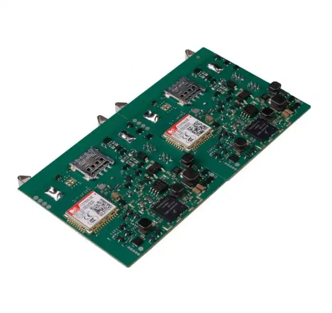
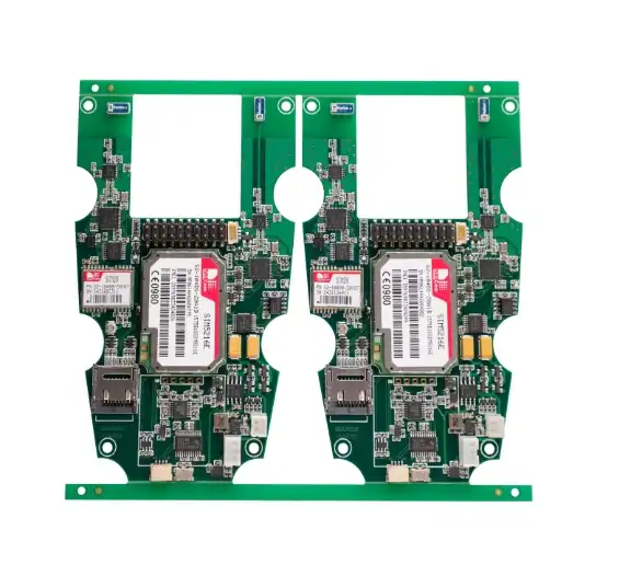
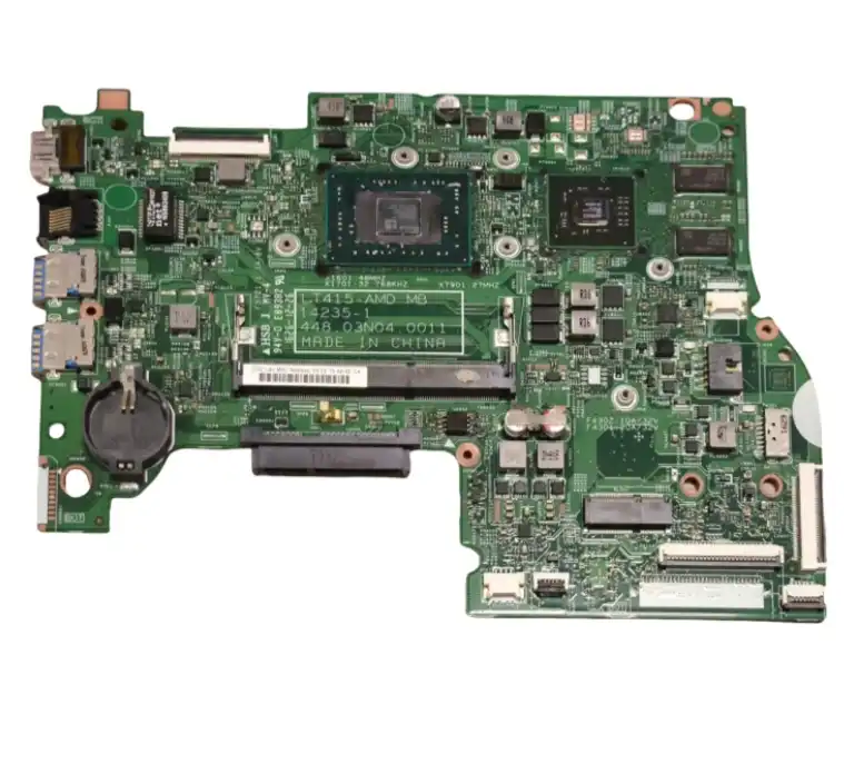
When it comes to assembling PCBs with complex components, precision is paramount. Modern PCB assembly services employ cutting-edge technologies to address the challenges posed by intricate circuit designs and miniaturized electronic parts. High-density boards require meticulous handling to ensure each component is placed and soldered accurately. Advanced automation, real-time quality inspection, and optimized reflow profiles collectively guarantee reliability, helping manufacturers meet the exacting standards of today’s electronic devices.
These machines utilize sophisticated vision systems and precision vacuum nozzles to accurately position components as small as 01005 or even 008004 packages. For BGAs and other area-array packages, specialized alignment tools and temperature-controlled reflow ovens ensure consistent solder joints. This precise assembly process minimizes solder bridging, enhances connectivity, and supports the long-term performance of high-speed and compact electronic assemblies.
Precision Placement and Soldering Methodologies
The complexity of modern PCBs demands exacting placement and soldering techniques. High-end PCB assembly services utilize laser-guided systems for component alignment, ensuring placement accuracy down to microns. For soldering, selective and vapor phase soldering techniques come into play, especially for heat-sensitive components or those requiring precise temperature control.
Vapor phase soldering, in particular, provides highly uniform heating and an oxygen-free environment, making it exceptionally suitable for complex, multi-layered PCBs with components that have differing thermal sensitivities. By immersing the board in a saturated vapor, heat is transferred evenly across all areas, minimizing hotspots and preventing warping. This method greatly reduces the risk of thermal shock and component damage, ensuring higher reliability and longer service life compared to conventional reflow soldering techniques.
Quality Assurance in Complex PCB Assembly
Quality assurance is a critical element in the assembly of complex PCBs. Advanced inspection and testing methodologies are essential to ensure the reliability and functionality of assembled boards. PCB assembly services specializing in complex components typically employ a multi-tiered inspection approach.
Automated Optical Inspection (AOI) systems use high-resolution cameras and sophisticated algorithms to detect issues like misalignments, solder bridges, or missing components. This technology is particularly valuable for inspecting dense, multi-layer boards where manual inspection would be impractical or error-prone.
X-ray and 3D Inspection Technologies
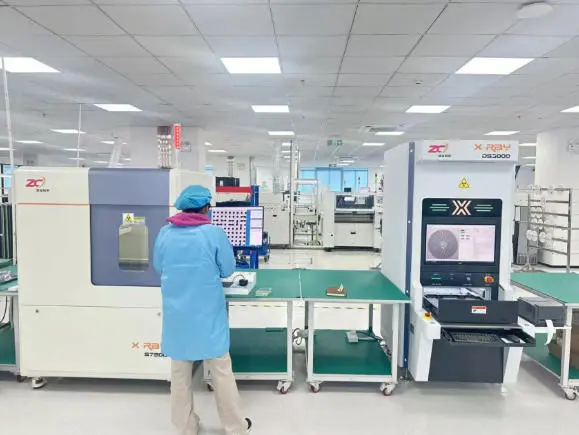
For components with hidden solder joints, such as BGAs or bottom-terminated components, X-ray inspection becomes indispensable. Advanced X-ray systems provide detailed images of solder connections beneath components, allowing technicians to identify voids, insufficient solder, or misalignments that would otherwise go undetected.

3D solder paste inspection (SPI) systems are another crucial tool in the quality assurance arsenal. These systems measure the volume, area, and height of solder paste deposits before component placement, ensuring that the right amount of solder is present for each joint. This preemptive measure significantly reduces defects in the final assembly.
Optimizing Design for Manufacturability (DFM)
Successful assembly of complex PCBs begins long before components touch the board. Design for Manufacturability (DFM) is a crucial process that bridges the gap between design intent and production realities. Experienced PCB assembly services often provide DFM feedback to optimize designs for the assembly process.
This collaborative approach involves analyzing the PCB layout for potential issues such as inadequate spacing between components, thermal management concerns, or areas where automated assembly might be challenging. By addressing these issues early in the design phase, manufacturers can significantly improve assembly yield and reliability.
Component Selection and Placement Strategies
The selection and placement of components play a vital role in optimizing PCB assembly. For complex designs, considerations such as thermal management, signal integrity, and power distribution become critical. Advanced PCB assembly services work closely with designers to recommend component choices that balance performance with manufacturability.
Strategic component placement is equally important. Grouping components with similar reflow profiles, minimizing the movement of the pick-and-place machine, and ensuring adequate space for inspection and rework are all strategies employed to enhance assembly efficiency and quality.
Conclusion
Optimizing PCB assembly for complex components is a multifaceted challenge that requires expertise, advanced technology, and meticulous attention to detail. By leveraging state-of-the-art PCB assembly services, manufacturers can ensure the reliable production of even the most complex designs. From precision placement and soldering to comprehensive quality assurance and thoughtful design optimization, each step in the process contributes to the overall success of the assembly.
As technology continues to advance, the demand for more complex and densely packed PCBs will only increase. Partnering with a skilled PCB assembly supplier or manufacturer who stays at the forefront of assembly techniques and technologies is crucial for companies looking to push the boundaries of what's possible in electronic design.
FAQ
What are the key challenges in assembling PCBs with complex components?
The main challenges include precise component placement, handling miniaturized parts, ensuring proper soldering of hidden joints, and maintaining overall board reliability.
How does automated optical inspection (AOI) contribute to complex PCB assembly?
AOI systems use high-resolution cameras and algorithms to detect issues like misalignments or solder bridges, crucial for inspecting dense, multi-layer boards.
Why is X-ray inspection important in complex PCB assembly?
X-ray inspection is vital for examining hidden solder joints in components like BGAs, allowing detection of voids or insufficient solder that would otherwise be invisible.
Advanced PCB Manufacturing Capabilities | Ring PCB
At Ring PCB, we excel in high-density stack-up manufacturing, producing 2-48 layer boards with advanced features like blind/buried vias and tight 3/3mil trace/spacing. Our smart manufacturing facility, equipped with LDI laser exposure and vacuum lamination, ensures precision adherence to IPC-6012 Class 3 standards. For complex PCB assembly needs, contact our expert team at [email protected]. As a leading PCB manufacturer, we offer comprehensive solutions for challenging designs in industries like 5G, automotive, and medical devices.
References
1. Johnson, R. (2022). Advanced Techniques in PCB Assembly for Complex Components. Journal of Electronics Manufacturing, 18(3), 245-260.
2. Chen, L., & Smith, K. (2021). Quality Assurance Methodologies in High-Density PCB Assembly. International Conference on Electronics Packaging (ICEP), 112-118.
3. Williams, T. (2023). Design for Manufacturability in Complex PCB Assemblies. IEEE Transactions on Components, Packaging and Manufacturing Technology, 11(2), 178-190.
4. Garcia, M., & Lee, S. (2022). Innovations in Automated Optical Inspection for High-Complexity PCBs. SMT: Surface Mount Technology, 37(9), 12-18.
5. Thompson, D. (2023). Thermal Management Strategies in Dense PCB Assemblies. Proceedings of the Thermal and Thermomechanical Phenomena in Electronic Systems, 234-241.


