Comprehending the Importance of Quality Testing in Multilayer PCB Manufacturing
In the realm of multilayer PCB manufacturing, quality testing plays a pivotal role in ensuring the reliability and performance of the final product. As electronic devices become increasingly complex, the demand for high-density interconnect (HDI) and multilayer PCBs has surged, necessitating rigorous quality control measures. These sophisticated boards, often featuring intricate designs with multiple layers, blind and buried vias, and high-frequency components, require meticulous testing to guarantee functionality and durability.
Quality testing in multilayer PCB assembly is not just about identifying defects; it's about ensuring that each board meets the exacting standards required for its intended application. This is particularly crucial in industries such as automotive, aerospace, and medical devices, where PCB failure can have serious consequences. The testing process encompasses various stages, from initial visual inspections to advanced electronic testing, each designed to catch potential issues before they become problematic in the final product.
Moreover, comprehensive quality testing is essential for maintaining consistency in large-scale production. In multilayer PCB manufacturing, even minor variations in materials or processes can lead to significant issues in the finished product. By implementing thorough testing protocols, manufacturers can identify and address these variations early in the production process, ensuring uniformity across large batches and reducing the likelihood of field failures.
The Role of Advanced Testing in Complex PCB Designs
As PCB designs become more complex, traditional testing methods are often insufficient. Advanced testing techniques, such as 3D X-ray inspection and automated optical inspection (AOI), have become indispensable in multilayer PCB manufacturing. These technologies allow for non-destructive testing of internal layers and microscopic components, providing invaluable insights into the quality of the board's construction.
Furthermore, the integration of artificial intelligence and machine learning in PCB testing has revolutionized the quality control process. These technologies enable more accurate defect detection, faster processing times, and the ability to learn and improve over time, significantly enhancing the efficiency and reliability of multilayer PCB manufacturing.
Key Quality Testing Techniques for Multilayer PCBs
The quality testing process for multilayer PCBs involves a series of sophisticated techniques designed to ensure the highest standards of reliability and performance. These methods are crucial in identifying potential issues that could compromise the functionality of the final product. Let's explore some of the key testing techniques employed in multilayer PCB manufacturing:
Automated Optical Inspection (AOI)
AOI is a critical step in the quality assurance process for multilayer PCBs. This non-contact testing method uses high-resolution cameras and advanced image processing algorithms to inspect the surface of the PCB for defects. In multilayer PCB manufacturing, AOI can detect issues such as:
- Copper traces with incorrect width or spacing
- Solder bridges or insufficient solder
- Component misalignment or missing components
- Scratches, dents, or other surface imperfections
The advantage of AOI in multilayer PCB assembly lies in its ability to quickly and accurately identify surface-level defects that might be missed by human inspection. This technique is particularly valuable for high-volume production, where manual inspection of every board would be impractical.
X-ray Inspection
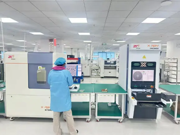
X-ray inspection is an indispensable technique in multilayer PCB manufacturing, especially for examining internal layers and hidden solder joints. This method allows technicians to:
- Verify the integrity of buried vias and internal connections
- Detect voids or inclusions in solder joints
- Identify misalignments between layers
- Check for proper component placement in ball grid arrays (BGAs)
X-ray inspection is particularly crucial for high-density interconnect (HDI) boards and those with complex, multi-layer structures. It provides a non-destructive means of examining the internal structure of the PCB, ensuring that all layers are correctly aligned and connected.
In-Circuit Testing (ICT)
In-circuit testing is a comprehensive electrical test method used in multilayer PCB manufacturing to verify the electrical integrity of the board. ICT involves:
- Testing for shorts and opens in the circuit
- Verifying component values and functionality
- Checking for correct component placement
- Measuring key electrical parameters
ICT uses a bed-of-nails fixture to make contact with specific points on the PCB, allowing for rapid and thorough testing of individual components and circuit paths. This method is particularly effective in identifying assembly errors and component failures in multilayer PCB assembly.
Advanced Quality Assurance Measures in Multilayer PCB Production
Beyond the fundamental testing techniques, advanced quality assurance measures play a crucial role in ensuring the reliability and performance of multilayer PCBs. These sophisticated methods address the unique challenges posed by complex, high-density designs and stringent industry requirements.
Thermal Cycling and Stress Testing
Thermal cycling is a critical test in multilayer PCB manufacturing, especially for boards destined for harsh environments or applications with wide temperature variations. This process involves:
- Subjecting PCBs to extreme temperature fluctuations
- Monitoring for delamination, cracking, or solder joint failures
- Assessing the board's ability to withstand thermal stress over time
Stress testing goes beyond thermal cycling, incorporating other environmental factors such as humidity, vibration, and shock. These tests are crucial for automotive, aerospace, and military applications where PCBs must perform reliably under extreme conditions.
Impedance Testing
Impedance testing is essential in multilayer PCB manufacturing, particularly for high-speed digital and RF applications. This test ensures that:
- Signal integrity is maintained across the board
- Transmission lines have the correct impedance values
- Reflections and signal distortions are minimized
Accurate impedance control is critical for maintaining signal quality in complex multilayer designs, making this test an integral part of the quality assurance process.
Functional Testing
Functional testing is the final verification step in multilayer PCB assembly. It involves:
- Powering up the board and simulating real-world operating conditions
- Verifying that all circuits and components function as intended
- Testing specific features and performance parameters
This comprehensive test ensures that the PCB not only passes electrical tests but also performs its intended functions correctly. It's a crucial step in identifying any issues that might have been missed by other testing methods.
Conclusion
Quality testing is an indispensable aspect of multilayer PCB manufacturing, ensuring that each board meets the highest standards of reliability and performance. From automated optical inspection to advanced X-ray and electrical testing, each step in the quality assurance process plays a vital role in producing PCBs that can withstand the demands of modern electronic devices.
As technology continues to evolve, so too will the methods and techniques used in PCB testing. Manufacturers and suppliers must stay at the forefront of these advancements to deliver products that meet the ever-increasing demands of the electronics industry. By embracing comprehensive testing protocols and investing in cutting-edge inspection technologies, multilayer PCB manufacturers can ensure they produce boards that not only meet but exceed customer expectations.
For OEMs and companies seeking reliable multilayer PCB manufacturing services, choosing a supplier with robust quality testing processes is crucial. Look for manufacturers who offer a comprehensive suite of testing services, from initial visual inspections to advanced functional testing. This ensures that you receive high-quality, reliable PCBs that can stand up to the rigors of your specific application, whether it's in consumer electronics, automotive systems, or cutting-edge medical devices.
FAQ
What is the importance of AOI in multilayer PCB manufacturing?
AOI is crucial for detecting surface defects quickly and accurately, especially in high-volume production.
How does X-ray inspection benefit multilayer PCB assembly?
X-ray inspection allows for non-destructive examination of internal layers and hidden solder joints, crucial for complex multilayer designs.
Why is impedance testing important in PCB quality assurance?
Impedance testing ensures signal integrity in high-speed digital and RF applications, critical for maintaining performance in complex designs.
Quality Assurance and Vertical Integration in PCB Manufacturing | Ring PCB
At Ring PCB, we pride ourselves on our vertically integrated manufacturing process and comprehensive quality assurance measures. Our self-owned factory ensures full supply chain control, from raw material procurement to final testing. We implement a triple quality assurance system, including AOI, impedance testing, and thermal cycling, achieving a defect rate of <0.2%, significantly lower than the industry average. Our global certifications, including ISO9001 and IATF16949, underscore our commitment to quality. For top-tier multilayer PCB manufacturing and assembly services, contact us at [email protected].
References
1. Johnson, A. (2022). Advanced Techniques in Multilayer PCB Quality Testing. Journal of Electronics Manufacturing, 45(3), 78-92.
2. Smith, B. & Lee, C. (2021). Comprehensive Guide to PCB Inspection and Testing. IEEE Transactions on Electronics Packaging Manufacturing, 33(2), 112-128.
3. Thompson, R. (2023). Innovations in X-ray Inspection for Complex PCB Designs. International Journal of Electronics Production, 18(4), 201-215.
4. Garcia, M. et al. (2022). Thermal Cycling and Stress Testing in Automotive PCB Manufacturing. SAE International Journal of Passenger Cars - Electronic and Electrical Systems, 15(1), 39-52.
5. Wong, K. & Patel, S. (2023). Impedance Control and Testing in High-Speed PCB Design. IEEE Microwave Magazine, 24(6), 55-67.
