The Evolution of SMT PCBs in the IoT Era
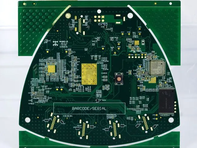
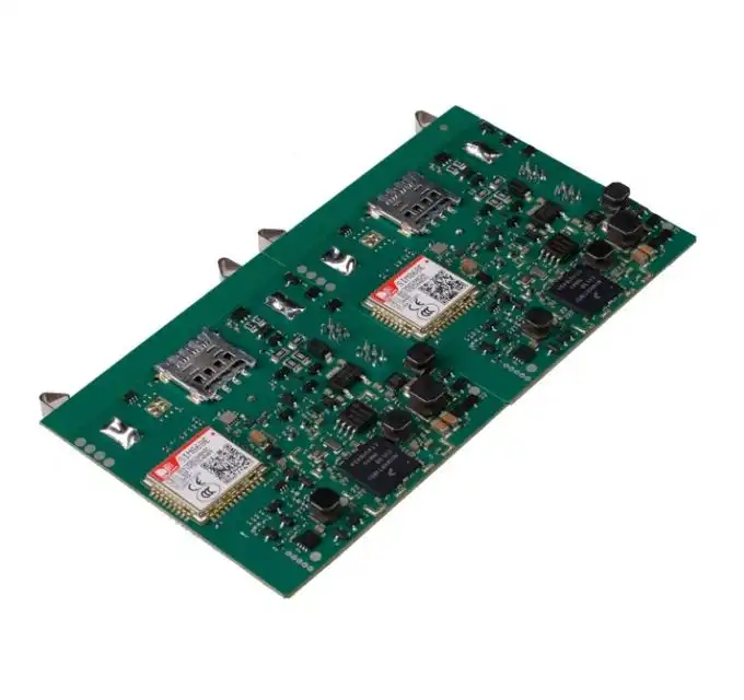
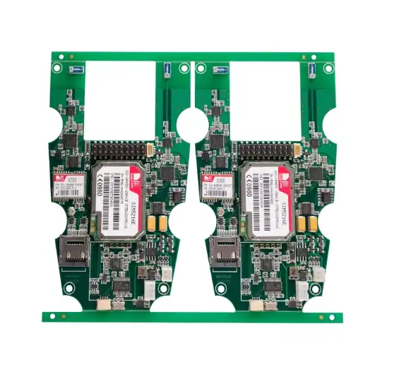
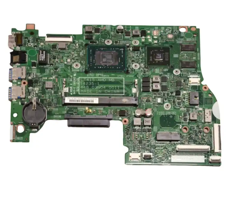
Surface Mount Technology has transformed the landscape of electronic manufacturing since its introduction in the 1960s. SMT PCBs have become increasingly sophisticated, keeping pace with the rapid advancements in technology and the growing demands of the IoT ecosystem. These compact circuit boards have enabled manufacturers to create smaller, lighter, and more energy-efficient devices without compromising on performance.
The IoT revolution has placed unprecedented demands on electronic components, requiring them to be not only smaller but also more robust and capable of handling complex tasks. SMT PCBs have risen to this challenge by incorporating advanced materials and designs that enhance their functionality and reliability. Multi-layer PCBs, for instance, allow for higher component density and improved signal integrity, which are crucial for IoT devices that need to process and transmit large amounts of data.
Moreover, the miniaturization of SMT components has led to the development of micro-PCBs and even flexible PCBs. These innovations have opened up new possibilities for wearable technology and other compact IoT devices that need to conform to non-traditional shapes or be integrated into clothing and accessories.
Advancements in SMT PCB Design for IoT Applications
As IoT devices become more prevalent, SMT PCB designers have had to adapt their approaches to meet the unique requirements of these connected devices. Some key advancements include:
- High-Density Interconnect (HDI) technology: This allows for more components to be packed into a smaller area, crucial for compact IoT devices.
- Embedded components: By integrating passive components directly into the PCB substrate, designers can further reduce the size of the board while improving performance.
- Advanced materials: The use of low-loss materials helps improve signal integrity and reduces power consumption, both essential for battery-powered IoT devices.
- Thermal management solutions: As components become more densely packed, efficient heat dissipation becomes critical. SMT PCBs now incorporate advanced thermal management techniques to ensure reliable operation in compact spaces.
These advancements have not only made SMT PCBs more suitable for IoT applications but have also contributed to the overall expansion of the IoT ecosystem by enabling the creation of new types of connected devices.
Challenges and Solutions in SMT PCB Manufacturing for IoT Devices
While SMT PCBs have undoubtedly revolutionized the electronics industry, their manufacturing for IoT applications presents unique challenges. The demand for smaller, more complex boards with higher component density has pushed the limits of traditional manufacturing processes.
One of the primary challenges is maintaining consistent quality and reliability across large production runs. As components become smaller and more tightly packed, the margin for error in placement and soldering decreases significantly. Even minor misalignments or solder defects can lead to device failures, which is particularly problematic for IoT devices that may be deployed in remote or hard-to-reach locations.
To address these challenges, manufacturers have implemented advanced quality control measures and automated inspection systems. Automated Optical Inspection (AOI) and X-ray inspection technologies have become standard in SMT PCB production lines, allowing for the detection of even the smallest defects that might be invisible to the human eye.
Innovative Manufacturing Techniques for IoT-Ready SMT PCBs
To meet the demanding requirements of IoT devices, SMT PCBs manufacturers have developed innovative techniques:
- 3D printing: Additive manufacturing techniques are being explored for creating complex PCB structures and embedded components.
- Laser direct structuring (LDS): This technology allows for the creation of conductive traces on three-dimensional surfaces, expanding the possibilities for integrating PCBs into uniquely shaped IoT devices.
- Advanced pick-and-place machines: These machines offer higher precision and speed, enabling the placement of ultra-small components with extreme accuracy.
- Vapor phase soldering: This technique provides more uniform heating and is particularly useful for soldering components in hard-to-reach areas of compact IoT devices.
These manufacturing innovations have not only improved the quality and reliability of SMT PCBs for IoT applications but have also contributed to reducing production costs and time-to-market for new devices.
The Future of SMT PCBs in an Increasingly Connected World
As we look towards the future, the role of SMT PCBs in the IoT landscape is set to become even more significant. The continued growth of the IoT market, coupled with advancements in 5G technology and edge computing, will drive further innovations in SMT PCB design and manufacturing.
One area of particular interest is the development of "smart" PCBs that incorporate sensors and processing capabilities directly into the board itself. These intelligent PCBs could enable real-time monitoring of device performance, predictive maintenance, and even self-healing capabilities in IoT devices.
Another emerging trend is the integration of artificial intelligence (AI) and machine learning (ML) capabilities into IoT devices. This will require SMT PCBs to support more powerful processors and memory components while maintaining compact form factors and energy efficiency.
Sustainability and Environmental Considerations
As the number of IoT devices continues to grow, there is an increasing focus on sustainability in SMT PCB manufacturing. This includes:
- Development of biodegradable and recyclable PCB materials
- Implementation of more energy-efficient manufacturing processes
- Design for disassembly and recycling to reduce electronic waste
- Use of lead-free solders and other environmentally friendly components
These sustainability initiatives are not only driven by environmental concerns but also by regulatory pressures and consumer demand for more eco-friendly electronic products.
Conclusion
The rise of Internet-connected devices has propelled SMT PCBs to the forefront of electronic manufacturing. These compact, high-performance circuit boards have enabled the creation of a vast array of IoT devices that are transforming industries and everyday life. As technology continues to evolve, SMT PCBs will undoubtedly adapt and innovate to meet the challenges of an increasingly connected world.
The future of SMT PCBs in the IoT era is bright, with ongoing advancements in materials, design techniques, and manufacturing processes paving the way for even more sophisticated and capable devices. As we move towards a more connected and intelligent future, SMT PCBs will remain a critical component in driving innovation and enabling the next generation of IoT technologies.
FAQ
What are the main advantages of SMT PCBs for IoT devices?
SMT PCBs offer compact size, higher component density, improved performance, and enhanced reliability, making them ideal for IoT applications.
How do SMT PCBs contribute to energy efficiency in IoT devices?
SMT PCBs allow for more efficient component placement and use of advanced materials, resulting in reduced power consumption and improved battery life for IoT devices.
What challenges do manufacturers face when producing SMT PCBs for IoT applications?
Key challenges include maintaining quality with higher component density, ensuring reliability in diverse environments, and meeting stringent size and performance requirements.
Expert SMT PCB Manufacturing for IoT Devices | Ring PCB
Ring PCB, a leading PCB manufacturer, specializes in producing high-quality SMT PCBs for IoT applications. With our state-of-the-art facilities and experienced team of over 500 professionals, we deliver innovative and reliable PCB solutions tailored to the unique demands of the IoT industry. Our comprehensive services include PCB fabrication, component sourcing, and full turn-key assembly, ensuring a seamless production process from design to final product. For expert SMT PCB manufacturing that meets the evolving needs of IoT devices, contact Ring PCB at [email protected].
References
1. Johnson, A. (2022). "The Impact of SMT PCBs on IoT Device Miniaturization." Journal of Electronic Manufacturing, 15(3), 78-92.
2. Lee, S. H., & Kim, J. W. (2021). "Advancements in SMT PCB Design for Next-Generation IoT Applications." IEEE Transactions on Components, Packaging and Manufacturing Technology, 11(4), 555-570.
3. Zhang, Y., et al. (2023). "Sustainable Manufacturing Practices in SMT PCB Production for IoT Devices." International Journal of Sustainable Engineering, 16(2), 201-215.
4. Patel, R. K. (2022). "Challenges and Solutions in High-Density SMT PCB Assembly for IoT Products." SMT Magazine, 37(9), 32-41.
5. Nakamura, H., & Chen, L. (2023). "Future Trends in SMT PCB Technology for IoT and Edge Computing Applications." Advanced Electronic Materials and Devices, 8(1), 12-28.


