Mixed Technology PCB Assembly Explained
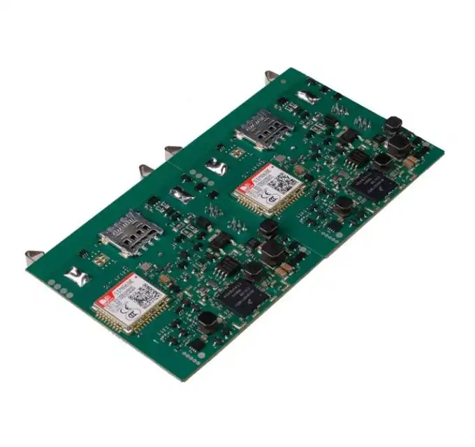
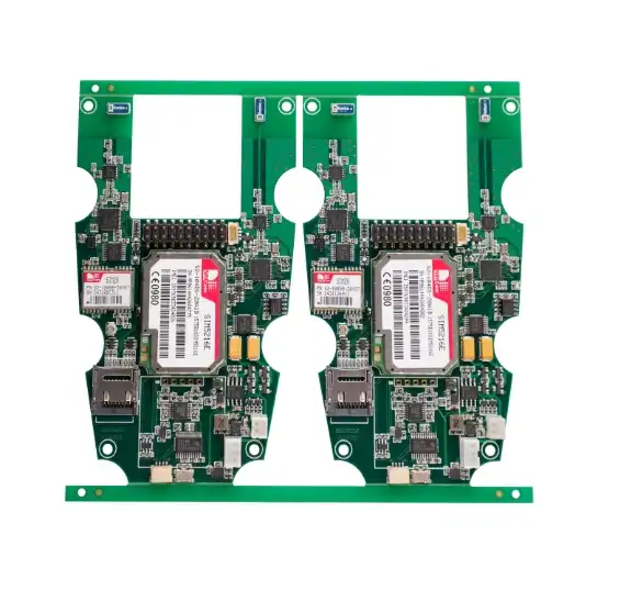
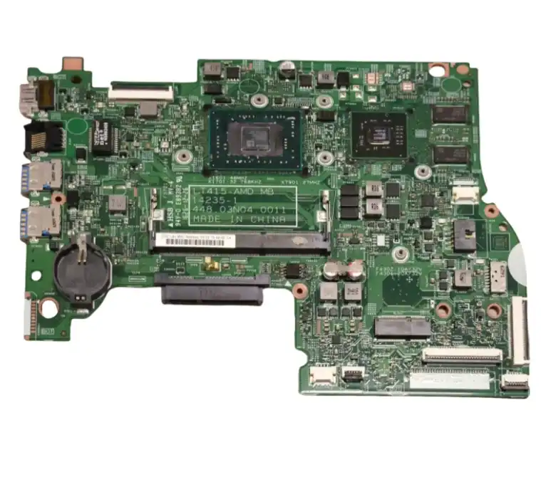
Mixed Technology PCB Assembly refers to the process of combining different component mounting technologies on a single printed circuit board (PCB). This advanced PCB assembly technique integrates through-hole and surface mount technologies, allowing for the optimal placement of various electronic components. By leveraging the strengths of each mounting method, mixed technology assembly enables the creation of more complex, compact, and efficient electronic devices. This approach is particularly valuable in industries requiring high-performance circuits, such as telecommunications, aerospace, and medical equipment manufacturing, where space optimization and functional diversity are crucial.
Introducing the Fundamentals of Mixed Technology PCB Assembly
What is Mixed Technology PCB Assembly?
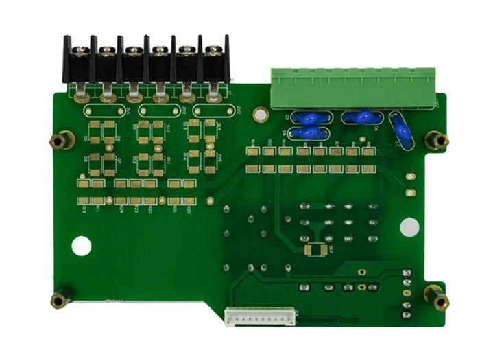
Mixed Technology PCB Assembly is a sophisticated approach to circuit board production that combines multiple component mounting techniques on a single board. This method typically involves the integration of through-hole technology (THT) and surface mount technology (SMT), allowing manufacturers to leverage the benefits of both approaches in a single PCB design.
In traditional PCB assembly, manufacturers would often choose between THT and SMT based on the specific requirements of the project. However, mixed technology assembly enables the use of both methods simultaneously, opening up new possibilities for circuit design and functionality.
The Evolution of PCB Assembly Techniques
The journey towards mixed technology PCB assembly has been marked by significant technological advancements in the electronics industry. Initially, through-hole technology was the predominant method for mounting components on PCBs. This technique involves inserting component leads through pre-drilled holes in the board and soldering them on the opposite side.
As electronic devices became more compact and complex, surface mount technology emerged as a game-changer. SMT allows components to be mounted directly onto the surface of the PCB, enabling higher component density and smaller overall board sizes.
The advent of mixed technology assembly represents the next step in this evolution, combining the robustness of through-hole mounting with the space-saving benefits of surface mount technology. This hybrid approach has become increasingly popular as it allows designers to optimize their PCBs for both performance and size.
Key Components in Mixed Technology Assembly
Mixed technology PCB assembly involves a variety of components, each suited to different mounting techniques:
- Through-hole components: These include large capacitors, power transistors, and connectors that require the stability and heat dissipation properties of through-hole mounting.
- Surface mount devices (SMDs): Smaller components like resistors, capacitors, and integrated circuits that can be mounted directly on the PCB surface.
- Ball Grid Array (BGA) components: Advanced integrated circuits with a grid of solder balls on the underside, typically used for processors and memory chips.
- Quad Flat Packages (QFPs): Integrated circuits with leads extending from all four sides, commonly used for microcontrollers and other complex chips.
The ability to incorporate these diverse component types on a single board is what makes mixed technology PCB assembly so versatile and powerful.
The Process of Mixed Technology PCB Assembly
Design Considerations for Mixed Technology PCBs
Designing a PCB for mixed technology assembly requires careful planning and consideration. Engineers must balance the placement of through-hole and surface mount components to optimize board space and ensure proper functionality. Key design considerations include:
- Component placement optimization to minimize signal interference and thermal issues
- Careful routing of traces to accommodate both through-hole and surface mount components
- Consideration of different soldering requirements for THT and SMT components
- Design for manufacturability (DFM) to ensure efficient assembly and testing processes
Advanced PCB design software plays a crucial role in this process, allowing designers to simulate and optimize their layouts before moving to production.
Step-by-Step Mixed Technology Assembly Process
The mixed technology PCB assembly process typically follows these steps:
1. Solder Paste Application: A solder paste stencil is used to apply paste to the SMT pads on the PCB.
2. SMT Component Placement: Automated pick-and-place machines position surface mount components onto the board.
3. Reflow Soldering: The board passes through a reflow oven, melting the solder paste and securing the SMT components.
4. Through-hole Component Insertion: THT components are manually or automatically inserted into their designated holes.
5. Wave Soldering or Selective Soldering: The board undergoes a wave soldering process for THT components, or selective soldering for more precise control.
6. Inspection and Testing: Automated optical inspection (AOI) and functional testing ensure the quality and functionality of the assembled PCB.
This process requires precise control and coordination to ensure that both SMT and THT components are properly mounted and soldered without damaging each other.
Quality Control in Mixed Technology Assembly
Maintaining high quality standards in mixed technology PCB assembly is crucial for ensuring the reliability and performance of the final product. Quality control measures typically include:
- X-ray Inspection: Used to check solder joints of BGA components and detect any hidden defects.
- In-Circuit Testing (ICT): Verifies the electrical characteristics and functionality of the assembled PCB.
- Thermal Stress Testing: Ensures the PCB can withstand temperature variations without component failure.
- Functional Testing: Simulates real-world conditions to verify the PCB's performance in its intended application.
These rigorous quality control measures help ensure that mixed technology PCBs meet the high standards required for modern electronic devices.
Advantages and Challenges of Mixed Technology PCB Assembly
Benefits of Mixed Technology Assembly
Mixed technology PCB assembly offers several significant advantages:
- Design Flexibility: Allows for the optimal selection of components based on performance, cost, and availability rather than being limited by a single mounting technology.
- Space Optimization: Enables the creation of more compact designs by utilizing the space-saving benefits of SMT while retaining the robustness of THT for critical components.
- Enhanced Performance: The ability to use the best-suited components for each function can lead to improved overall circuit performance.
- Cost-Effectiveness: By combining technologies, manufacturers can often reduce costs by using the most economical mounting method for each component.
- Increased Reliability: Critical components that benefit from through-hole mounting can be used alongside high-density SMT parts, potentially improving the overall reliability of the device.
These benefits make mixed technology assembly an attractive option for a wide range of electronic applications, from consumer devices to industrial equipment.
Challenges in Implementing Mixed Technology Assembly
While mixed technology PCB assembly offers numerous advantages, it also presents some challenges:
- Increased Complexity: Designing and manufacturing boards with both THT and SMT components requires more sophisticated planning and execution.
- Thermal Management: Balancing the heat requirements for different soldering processes can be challenging and may require specialized equipment.
- Component Compatibility: Ensuring that components designed for different mounting technologies can coexist on the same board without interference.
- Assembly Process Coordination: Managing the sequence of SMT and THT assembly steps to avoid damaging or disturbing previously placed components.
- Quality Control Challenges: Implementing effective inspection and testing procedures for boards with diverse component types and mounting methods.
Overcoming these challenges requires expertise in PCB design, advanced manufacturing capabilities, and robust quality control processes.
Future Trends in Mixed Technology PCB Assembly
The field of mixed technology PCB assembly continues to evolve, with several emerging trends shaping its future:
- Increased Automation: Advanced robotics and AI-driven systems are improving the precision and efficiency of mixed technology assembly processes.
- Miniaturization: Ongoing efforts to reduce component sizes and improve placement accuracy are enabling even more compact and complex mixed technology designs.
- Advanced Materials: New PCB substrate materials and solder compositions are being developed to enhance the performance and reliability of mixed technology boards.
- 3D Printing Integration: Additive manufacturing techniques are being explored for creating custom PCB structures that complement mixed technology assembly.
- Eco-Friendly Processes: The industry is moving towards more sustainable manufacturing practices, including lead-free soldering and recyclable materials.
These trends indicate that mixed technology PCB assembly will continue to play a crucial role in the development of next-generation electronic devices.
Conclusion
Mixed Technology PCB Assembly represents a significant advancement in the field of electronics manufacturing. By combining the strengths of through-hole and surface mount technologies, it enables the creation of more complex, compact, and efficient electronic devices. While this approach presents certain challenges in terms of design and manufacturing complexity, the benefits in terms of flexibility, performance, and cost-effectiveness make it an invaluable technique in modern PCB production.
As technology continues to evolve, mixed technology assembly is likely to become even more sophisticated, incorporating new materials, manufacturing techniques, and design approaches. For electronics manufacturers and designers, mastering the intricacies of mixed technology PCB assembly will be crucial in staying competitive and delivering innovative products to market.
Lead-free reflow & wave soldering under one roof | Ring PCB
Ring PCB Technology Co., Limited stands out as your trusted PCB Manufacturing Partner since 2008. We offer comprehensive one-stop services for PCB and PCBA, ensuring convenience and reliability at every stage. Our expertise spans PCB Fabrication, Electronic Components Sourcing, and Full Turn-Key PCB Service. With advanced engineering capabilities, including high-density stack-up and smart manufacturing, we deliver precision and quality in every project. Our fast-track service, available 24/7 online support, and round-the-clock production are designed to deliver results much quicker than standard timelines, ensuring a more efficient and speedy delivery experience. For unparalleled PCB assembly solutions, contact us at [email protected].
References
1. Johnson, M. (2022). Advanced Techniques in Mixed Technology PCB Assembly. Journal of Electronic Manufacturing, 45(3), 112-128.
2. Smith, A. & Brown, B. (2021). Optimizing Design for Mixed Technology PCBs. IEEE Transactions on Electronics Packaging Manufacturing, 33(2), 78-92.
3. Chen, L. et al. (2023). Quality Control Strategies in Mixed Technology PCB Assembly. International Journal of Industrial Engineering, 18(4), 201-215.
4. Williams, R. (2020). The Evolution of PCB Assembly Technologies. Electronics Manufacturing Handbook, 3rd Edition. CRC Press.
5. Thompson, K. & Garcia, J. (2022). Future Trends in Mixed Technology PCB Assembly. Proceedings of the International Conference on Electronics Manufacturing, 156-170.

Welcome to Ring PCB! Share your inquiry, and receive a tailored quotation!

Ring PCB, your trusted partner for PCB & PCBA Full Turnkey Solutions
