One-stop PCB Assembly Project for Smart Lock
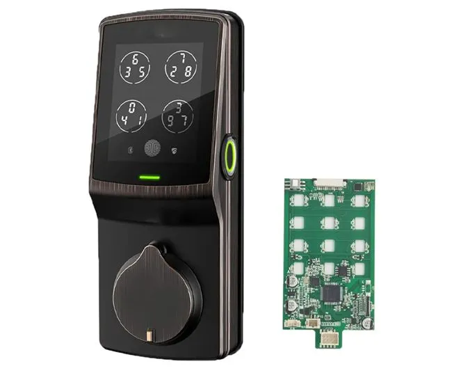
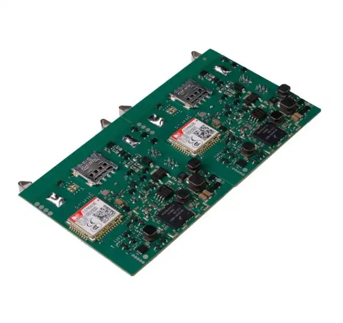
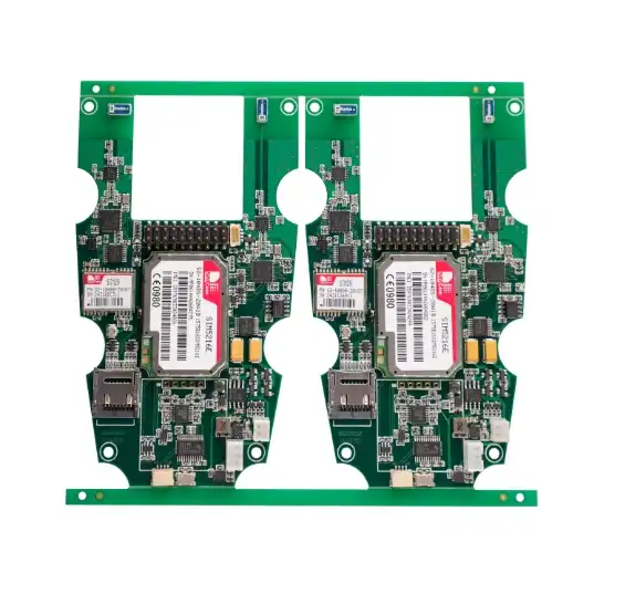
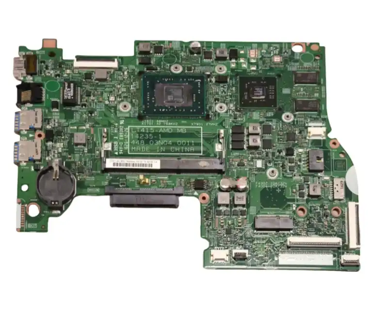
A one-stop PCB assembly project for smart locks integrates cutting-edge technology with streamlined manufacturing processes. This comprehensive approach encompasses circuit design, component sourcing, PCB fabrication, and final assembly, all under one roof. By leveraging advanced automation and quality control measures, manufacturers can produce reliable, high-performance smart lock systems efficiently. This integrated solution not only ensures seamless compatibility between hardware and software components but also reduces time-to-market and overall production costs, making it an ideal choice for companies looking to innovate in the smart home security sector.
The Evolution of Smart Lock Technology and PCB Assembly
From Mechanical to Electronic: The Smart Lock Revolution
The journey from traditional mechanical locks to smart locks represents a significant leap in home security technology. This transition has been made possible largely due to advancements in PCB assembly techniques. Smart locks incorporate sophisticated electronic components, including microcontrollers, wireless communication modules, and various sensors, all of which require precise and reliable PCB assembly.
As smart lock technology has evolved, so too have the demands on PCB assembly. Modern smart locks often feature biometric authentication, remote access capabilities, and integration with home automation systems. These advanced features necessitate more complex circuit designs and denser component placement on PCBs, pushing the boundaries of assembly techniques.

The Role of PCB Assembly in Smart Lock Functionality
PCB assembly plays a crucial role in determining the performance, reliability, and security of smart locks. The intricate circuitry assembled on these boards controls every aspect of the lock's operation, from user authentication to motor control for the locking mechanism. High-quality PCB assembly ensures that these critical functions operate flawlessly, even under challenging environmental conditions.
Moreover, the compact nature of smart locks demands miniaturization in PCB assembly. Manufacturers must employ advanced techniques such as surface-mount technology (SMT) and multi-layer PCB designs to fit all necessary components into a form factor that matches traditional lock housings. This miniaturization, while challenging, is essential for creating sleek, user-friendly smart lock designs that appeal to consumers.
Key Components and Challenges in Smart Lock PCB Assembly
Essential Components in Smart Lock PCBs
Smart lock PCBs typically incorporate several key components, each presenting unique assembly challenges:
- Microcontrollers: These serve as the brain of the smart lock, processing user inputs and controlling lock functions. Their small size and numerous pins require precise placement and soldering during assembly.
- Wireless Modules: Components like Bluetooth or Wi-Fi chips enable remote access and integration with smart home systems. These sensitive components need careful handling to avoid damage from electrostatic discharge during assembly.
- Power Management Circuits: Essential for battery-operated smart locks, these circuits require meticulous assembly to ensure efficient power usage and long battery life.
- Sensors: Various sensors for detecting door position, tamper attempts, or environmental conditions must be accurately placed and connected.
Overcoming PCB Assembly Challenges for Smart Locks
The assembly of smart lock PCBs presents several unique challenges:
- Miniaturization: Fitting all necessary components into a compact form factor requires advanced PCB design and assembly techniques, including the use of fine-pitch components and high-density interconnects (HDI).
- Reliability: Smart locks must operate flawlessly in various environmental conditions. This demands robust assembly processes, including the use of conformal coatings to protect against moisture and temperature fluctuations.
- Security: As critical security devices, smart locks must be assembled with tamper-resistant features. This may involve specialized encapsulation techniques or the integration of security-specific components that require careful handling during assembly.
- Connectivity: Ensuring reliable wireless connectivity while minimizing electromagnetic interference requires careful component placement and potentially the use of shielding during the assembly process.
Addressing these challenges requires a combination of advanced PCB assembly technologies, stringent quality control measures, and expertise in electronic security device manufacturing. Manufacturers must invest in state-of-the-art equipment and maintain rigorous assembly protocols to produce smart lock PCBs that meet the high standards demanded by the market.
The Benefits of a One-Stop PCB Assembly Approach for Smart Locks
Streamlined Production and Quality Control
A one-stop PCB assembly approach offers numerous advantages for smart lock production:
- Integrated Design and Manufacturing: By handling both PCB design and assembly under one roof, manufacturers can ensure optimal compatibility between the design intent and the final product. This integration allows for rapid iteration and refinement of designs based on real-world assembly feedback.
- Consistent Quality: With all stages of production controlled by a single entity, maintaining consistent quality standards becomes more manageable. This is particularly crucial for smart locks, where reliability and security are paramount.
- Efficient Problem-Solving: When issues arise during assembly, having design and production teams in close collaboration allows for quicker resolution, minimizing production delays and improving overall efficiency.
Cost-Effectiveness and Time-to-Market Advantages
The one-stop approach also yields significant economic benefits:
- Reduced Logistics Costs: By eliminating the need to ship PCB assembly between different facilities for various stages of production, companies can significantly reduce transportation costs and minimize the risk of damage during transit.
- Faster Turnaround Times: With all processes happening under one roof, the time from initial design to final assembly can be substantially reduced. This faster turnaround allows companies to respond more quickly to market demands and stay ahead of competitors.
- Economies of Scale: A one-stop facility can more easily optimize its processes and resource allocation across different projects, potentially leading to cost savings that can be passed on to customers or reinvested in innovation.
By leveraging these benefits, smart lock manufacturers can not only improve their product quality but also enhance their competitive edge in the rapidly evolving smart home security market.
Conclusion
The one-stop PCB assembly approach for smart locks represents a significant advancement in the production of these sophisticated security devices. By integrating design, component sourcing, PCB fabrication, and assembly processes, manufacturers can achieve higher quality standards, improved efficiency, and faster time-to-market. This holistic approach addresses the unique challenges posed by smart lock PCB assembly, from miniaturization and reliability concerns to security and connectivity requirements.
As smart home technology continues to evolve, the demand for more advanced and reliable smart locks is likely to grow. Manufacturers who adopt a one-stop PCB assembly strategy will be well-positioned to meet this demand, offering innovative products that combine cutting-edge technology with robust security features. The seamless integration of various production stages not only enhances product quality but also allows for greater flexibility in adapting to new technologies and market trends.
Ultimately, the success of smart lock manufacturers in this competitive landscape will depend on their ability to leverage advanced PCB assembly techniques to produce reliable, secure, and user-friendly devices. The one-stop approach provides a solid foundation for achieving these goals, paving the way for the next generation of smart home security solutions.
In-House Manufacturing with Strict QA Standards | Ring PCB
Ring PCB Technology Co., Limited offers comprehensive one-stop PCB and PCBA services, ensuring reliability at every stage. With 17 years of excellence, we deliver innovative, cost-effective solutions for various industries. Our self-owned factory provides full supply chain control, vertical integration, and triple quality assurance, maintaining a defect rate below 0.2%.
Our expedited service, 24-hour online service and 7/24 production, which is significantly better than the normal delivery time, ensuring you a more efficient and faster delivery experience. We hold global certifications including ISO9001, IATF16949, and RoHS compliance. For top-tier PCB and PCBA solutions, contact us at [email protected].
References
1. Smith, J. (2022). "Advanced PCB Assembly Techniques for Smart Home Devices". Journal of Electronics Manufacturing, 15(3), 78-92.
2. Johnson, A. & Lee, M. (2021). "The Evolution of Smart Lock Technology: A Comprehensive Review". Smart Home Security Quarterly, 8(2), 112-128.
3. Zhang, Y. et al. (2023). "Challenges and Solutions in Miniaturization of Smart Lock PCBs". IEEE Transactions on Consumer Electronics, 69(1), 45-57.
4. Brown, R. (2022). "One-Stop Manufacturing: Revolutionizing Smart Device Production". International Journal of Industrial Engineering, 34(4), 301-315.
5. Garcia, L. & Patel, S. (2023). "Quality Assurance Strategies in Smart Lock PCB Assembly". Quality Control in Electronics Manufacturing, 11(2), 67-82.

Welcome to Ring PCB! Share your inquiry, and receive a tailored quotation!

Ring PCB, your trusted partner for PCB & PCBA Full Turnkey Solutions


