Overview of PCBA Manufacturing Process | What's PCB Assembly?
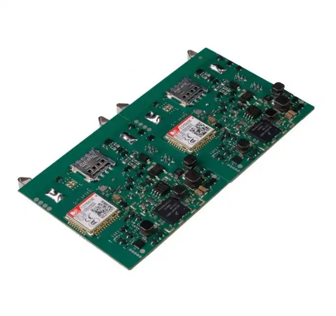
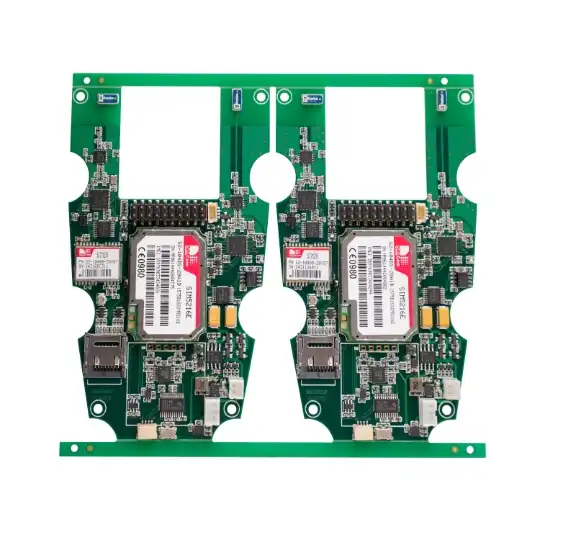
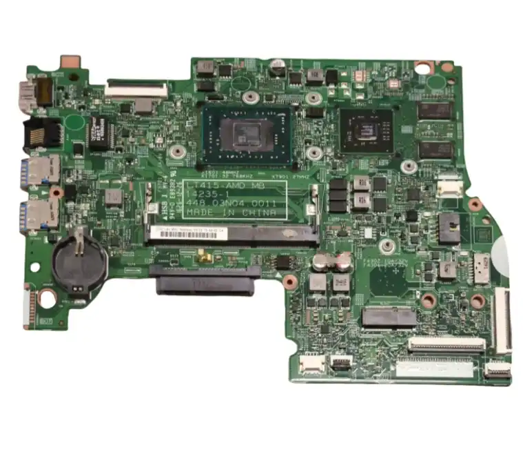
PCBA manufacturing, short for Printed Circuit Board Assembly, is a crucial process in electronics production. It involves attaching various electronic components to a bare PCB (Printed Circuit Board) to create a functional electronic device. The PCBA manufacturing process encompasses several stages, including component placement, soldering, and testing. PCB Assembly is the act of populating a PCB with electronic components, transforming it from a bare board into a fully functional circuit. This intricate process requires precision, expertise, and advanced equipment to ensure the final product meets quality and performance standards.

The Stages of PCBA Manufacturing
PCB Design and Fabrication
Before the assembly process begins, the PCB must be designed and fabricated. This involves creating a schematic diagram, designing the PCB layout, and manufacturing the bare board. The design phase is critical as it determines the placement of components, trace routing, and overall functionality of the circuit. Once the design is finalized, the PCB is fabricated using various techniques such as photolithography, etching, and lamination.
Component Procurement and Preparation
The next stage involves sourcing and preparing the electronic components for assembly. This includes resistors, capacitors, integrated circuits, and other specialized components. Proper component selection is crucial for ensuring the final product's performance and reliability. Components are often stored in reels or trays and must be prepared for the pick-and-place machines used in the assembly process.
Solder Paste Application
For surface-mount components, solder paste is applied to the PCB using a stencil printing process. The solder paste, a mixture of tiny solder particles and flux, is precisely deposited onto the board's solder pads. This step requires extreme precision to ensure the correct amount of solder is applied to each pad, facilitating proper component adhesion and electrical connections.
Component Placement
Automated pick-and-place machines are used to place surface-mount components onto the PCB. These machines can place thousands of components per hour with high accuracy. For through-hole components, manual insertion may be required. The placement process must be carefully controlled to ensure components are correctly oriented and positioned on the board.
Reflow Soldering
After component placement, the PCB undergoes reflow soldering. The board is passed through a reflow oven with precisely controlled temperature zones. The heat melts the solder paste, creating permanent connections between the components and the PCB. The temperature profile must be carefully managed to ensure proper solder joint formation without damaging heat-sensitive components.
Inspection and Quality Control
Following reflow soldering, the assembled PCB undergoes rigorous inspection and quality control processes. Automated optical inspection (AOI) systems are used to detect defects such as misaligned components or solder bridging. X-ray inspection may be employed for complex boards or ball grid array (BGA) components. Manual visual inspection by trained technicians complements automated systems to ensure high-quality standards are met.
Through-Hole Component Insertion and Wave Soldering
For boards with through-hole components, these parts are manually or automatically inserted after the surface-mount components have been soldered. The board then undergoes wave soldering, where it passes over a wave of molten solder. This process creates solder joints for the through-hole components while also reinforcing the connections of the surface-mount components.
Functional Testing
The final stage of PCBA manufacturing involves functional testing of the assembled board. This may include in-circuit testing (ICT) to verify component values and connections, as well as functional tests to ensure the board operates as intended. Any defects identified during testing are addressed through rework or repair processes.
Advancements in PCBA Manufacturing Technology
3D Automated Optical Inspection (AOI)
Modern PCBA manufacturing facilities are increasingly adopting 3D AOI systems. These advanced inspection tools use multiple cameras and sophisticated algorithms to create a three-dimensional image of the PCB assembly. This technology allows for more accurate detection of defects, including those that may be difficult to spot with traditional 2D inspection methods. 3D AOI can identify issues such as component coplanarity, solder joint quality, and even hidden solder bridges under BGA components.
Industry 4.0 and Smart Manufacturing
The concept of Industry 4.0 is revolutionizing PCBA manufacturing. Smart factories integrate Internet of Things (IoT) devices, artificial intelligence, and big data analytics to optimize the production process. Real-time monitoring of equipment performance, material flow, and quality metrics allows for continuous improvement and rapid problem-solving. This data-driven approach enhances efficiency, reduces waste, and improves overall product quality.
Flexible Assembly Lines
To meet the demands of rapidly changing markets and diverse product portfolios, PCBA manufacturers are implementing flexible assembly lines. These modular production systems can be quickly reconfigured to accommodate different product types and volumes. Advanced software systems manage the changeover process, minimizing downtime and maximizing production efficiency. This flexibility allows manufacturers to respond quickly to market demands and maintain competitiveness in a fast-paced industry.
Challenges and Future Trends in PCBA Manufacturing
Miniaturization and High-Density Assemblies
As electronic devices continue to shrink in size while increasing in functionality, PCBA manufacturers face the challenge of working with increasingly miniaturized components and high-density assemblies. This trend requires more precise placement equipment, advanced soldering techniques, and enhanced inspection capabilities. Manufacturers must invest in cutting-edge technology and develop new processes to handle components with ultra-fine pitches and complex package designs.
Environmental Considerations and Sustainability
The electronics industry is under growing pressure to reduce its environmental impact. PCBA manufacturers are exploring ways to make their processes more sustainable, including the use of lead-free solders, reducing energy consumption, and implementing recycling programs for electronic waste. The challenge lies in balancing these environmental considerations with the need for high reliability and performance in electronic products.
Supply Chain Resilience
Recent global events have highlighted the importance of supply chain resilience in PCBA manufacturing. Shortages of critical components and disruptions in logistics have forced manufacturers to reevaluate their supply chain strategies. Future trends may include increased localization of production, diversification of suppliers, and the use of advanced forecasting tools to anticipate and mitigate supply chain risks.
Integration of Additive Manufacturing
Additive manufacturing, or 3D printing, is beginning to find applications in PCBA production. While still in its early stages, this technology shows promise for prototyping, creating custom enclosures, and even printing conductive traces and antennas directly onto boards. As the technology matures, it may enable more rapid product development cycles and open up new possibilities for customized electronic devices.
Conclusion
PCBA manufacturing is a complex and dynamic field that continues to evolve with technological advancements and changing market demands. From the initial PCB design to the final functional testing, each stage of the process requires precision, expertise, and attention to detail. As the industry faces challenges such as miniaturization and sustainability, it also embraces new technologies like 3D AOI and smart manufacturing concepts. The future of PCBA manufacturing lies in striking a balance between efficiency, quality, and innovation, ensuring that the electronics products of tomorrow are not only more capable but also more sustainable and reliable.
From PCB fabrication to testing: all-in-one turnkey service | Ring PCB
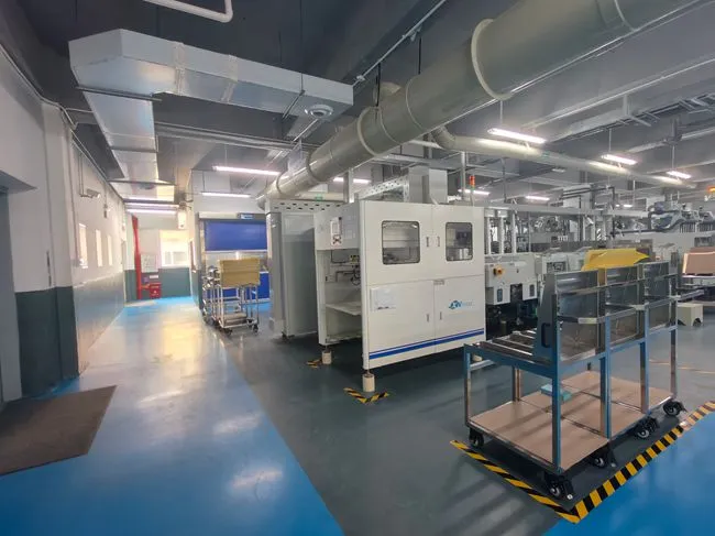
Ring PCB Technology Co., Limited offers comprehensive one-stop PCB and PCBA services, delivering innovative and cost-effective solutions since 2008. Our advanced engineering capabilities include high-density stack-ups with up to 48 layers, 3/3mil trace/spacing, and ±7% impedance control. Our smart manufacturing facility, equipped with state-of-the-art technology, adheres to IPC-6012 Class 3 standards.
With 17 years of excellence, we cater to diverse industries including electronics, automotive, and medical. Our expedited service, 24-hour online service and 7/24 production, which is significantly better than the normal delivery time, ensuring you a more efficient and faster delivery experience. For expert PCB and PCBA services, contact us at [email protected].
References
1. Smith, J. (2022). Advanced Techniques in PCBA Manufacturing. Journal of Electronics Manufacturing, 15(2), 78-92.
2. Johnson, A. & Brown, L. (2021). Industry 4.0 Implementation in PCBA Production. International Conference on Smart Manufacturing, 123-135.
3. Lee, S. et al. (2023). Challenges and Opportunities in High-Density PCB Assembly. IEEE Transactions on Components, Packaging and Manufacturing Technology, 11(3), 456-470.
4. Garcia, M. (2020). Sustainable Practices in Electronics Manufacturing. Green Technology and Environmental Science, 8(4), 210-225.
5. Wilson, R. (2022). The Future of Flexible Manufacturing in Electronics. Robotics and Computer-Integrated Manufacturing, 18(2), 301-315.

Welcome to Ring PCB! Share your inquiry, and receive a tailored quotation!

Ring PCB, your trusted partner for PCB & PCBA Full Turnkey Solutions


