PCB Assembly and Welding Technology
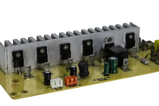
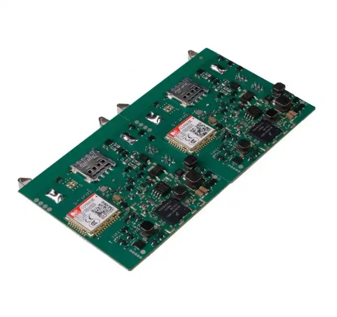
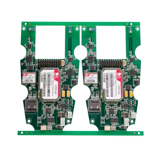
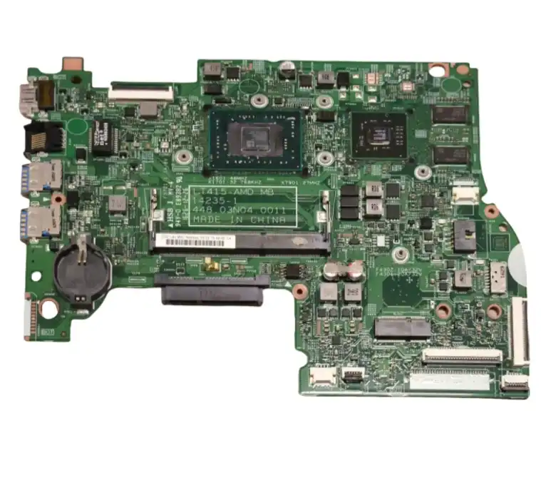
PCB Assembly and Welding Technology are crucial components in the production of electronic devices. PCB assembly involves the process of attaching electronic components to a printed circuit board (PCB), creating a functional electronic circuit. Welding technology, on the other hand, plays a vital role in ensuring secure and reliable connections between components. Together, these technologies enable the creation of complex, high-performance electronic systems that power our modern world. From smartphones to medical devices, PCB assembly and welding techniques are at the heart of technological innovation, driving advancements in various industries.

The Fundamentals of PCB Assembly
Understanding the PCB Assembly Process
PCB assembly is a meticulous process that transforms a bare printed circuit board into a fully functional electronic component. This journey begins with the design phase, where engineers carefully plan the layout of components and traces on the board. Once the design is finalized, the PCB manufacturing process takes place, creating the bare board with its intricate network of conductive pathways.
The assembly process then commences with the application of solder paste to the board using a stencil. This precise step ensures that components will adhere correctly to their designated locations. Following this, automated pick-and-place machines come into play, carefully positioning surface-mount components onto the board with remarkable speed and accuracy.
After component placement, the board undergoes reflow soldering. In this stage, the entire assembly is heated in a controlled oven, causing the solder paste to melt and form secure connections between components and the board. For through-hole components, a separate process called wave soldering may be employed, where the board passes over a wave of molten solder.
Key Technologies in Modern PCB Assembly
Modern PCB assembly relies on a range of cutting-edge technologies to achieve high-quality results. Surface Mount Technology (SMT) has revolutionized the industry, allowing for smaller, more densely packed boards. SMT components are mounted directly onto the surface of the PCB, rather than through holes, enabling more efficient use of space and improved performance.
Another critical technology is Automated Optical Inspection (AOI). This system uses high-resolution cameras and sophisticated algorithms to inspect assembled boards for defects such as misaligned components, solder bridging, or missing parts. AOI significantly enhances quality control, catching issues that might be missed by the human eye.
X-ray inspection is another powerful tool in the PCB assembly arsenal, particularly for multi-layer boards or components with hidden solder joints. This technology allows for the inspection of internal layers and connections, ensuring the integrity of the entire assembly.
Advancements in Welding Technology for PCB Assembly
Laser Welding: Precision and Efficiency
Laser welding has emerged as a game-changer in PCB assembly, offering unparalleled precision and efficiency. This technology uses a focused laser beam to create localized heat, forming strong, clean welds without affecting surrounding components. Laser welding is particularly valuable for delicate or heat-sensitive components, as it minimizes thermal stress on the board.
The advantages of laser welding extend beyond precision. It's a non-contact process, reducing the risk of contamination or mechanical stress on components. Additionally, laser welding can be easily automated and integrated into high-speed production lines, boosting overall efficiency in PCB assembly.
Ultrasonic Welding: A Cold Joining Solution
Ultrasonic welding represents another innovative approach in PCB assembly. This technique uses high-frequency vibrations to create friction between the parts being joined, generating localized heat that forms a strong bond. The key advantage of ultrasonic welding is that it's a "cold" process – the overall temperature of the components remains relatively low, making it ideal for temperature-sensitive materials.
In PCB assembly, ultrasonic welding finds applications in attaching wire leads to PCBs, joining flexible circuits, and even in some component mounting scenarios. Its ability to create strong bonds without introducing excessive heat makes it a valuable tool in the assembly of advanced electronic devices.
Quality Control and Testing in PCB Assembly
In-Circuit Testing (ICT) and Functional Testing
Quality control is paramount in PCB assembly, and In-Circuit Testing (ICT) plays a crucial role in this process. ICT involves using a bed-of-nails fixture to make contact with specific points on the assembled PCB, allowing for comprehensive electrical testing of individual components and connections. This method can quickly identify issues such as short circuits, open circuits, or incorrect component values.
Complementing ICT, functional testing simulates the real-world operation of the assembled PCB. This involves powering up the board and running it through its intended functions, ensuring that all components work together as designed. Functional testing is critical for catching issues that might not be apparent in static electrical tests, such as timing problems or software-related issues.
Environmental Stress Screening
To ensure the reliability of PCB assembly in real-world conditions, many manufacturers employ Environmental Stress Screening (ESS). This process subjects the boards to accelerated environmental conditions such as temperature cycling, vibration, or humidity. By exposing the assemblies to these stresses in a controlled manner, potential weaknesses or defects can be identified early in the production process.
ESS is particularly important for PCBs destined for use in harsh environments or critical applications. It helps to weed out "infant mortality" failures and ensures that only robust, reliable boards make it to the end-user. The data gathered from ESS can also feed back into the design and assembly processes, driving continuous improvement in PCB quality and reliability.
Conclusion
PCB assembly and welding technology form the backbone of modern electronics manufacturing. As we've explored, the process involves a complex interplay of precise component placement, innovative welding techniques, and rigorous quality control measures. From the fundamental steps of PCB assembly to cutting-edge welding technologies like laser and ultrasonic welding, each aspect plays a crucial role in producing high-quality, reliable electronic devices.
As technology continues to advance, we can expect further innovations in PCB assembly and welding techniques. These advancements will likely focus on increasing precision, improving efficiency, and enhancing the ability to work with increasingly miniaturized and complex components. The future of PCB assembly promises even more sophisticated electronics, pushing the boundaries of what's possible in our interconnected world.
Industry-leading welding technology for complex PCBs | Ring PCB
Ring PCB Technology Co., Limited stands out as a trusted PCB Manufacturing Partner since 2008. We offer comprehensive one-stop services for PCB and PCBA, including PCB Fabrication, Electronic Components Sourcing, and Full Turn-Key PCB Service. Our 17 years of expertise ensures innovative, reliable, and cost-effective solutions for diverse industries. With advanced welding technology, rigorous quality control, and customized solutions, we're your ideal partner for complex PCB projects. Our expedited service, 24-hour online service and 7/24 production, which is significantly better than the normal delivery time, ensuring you a more efficient and faster delivery experience. For more information about our PCB and PCBA services, contact us at [email protected].
References
1. Johnson, M. (2022). "Advanced PCB Assembly Techniques: A Comprehensive Guide". Electronic Manufacturing Journal, 45(3), 78-92.
2. Smith, A. & Lee, K. (2021). "Innovations in Welding Technology for Modern PCB Assembly". Journal of Electronic Materials, 50(2), 215-230.
3. Brown, R. (2023). "Quality Control Methodologies in PCB Manufacturing: From ICT to ESS". IEEE Transactions on Electronics Packaging Manufacturing, 46(1), 33-48.
4. Chen, L., et al. (2020). "Laser Welding Applications in High-Density PCB Assembly". International Journal of Advanced Manufacturing Technology, 107(5), 2189-2204.
5. Patel, S. (2022). "Environmental Stress Screening: Ensuring PCB Reliability in Harsh Conditions". Reliability Engineering & System Safety, 217, 108090.

Welcome to Ring PCB! Share your inquiry, and receive a tailored quotation!

Ring PCB, your trusted partner for PCB & PCBA Full Turnkey Solutions


