Understanding PCBA BGA Assembly and Its Applications
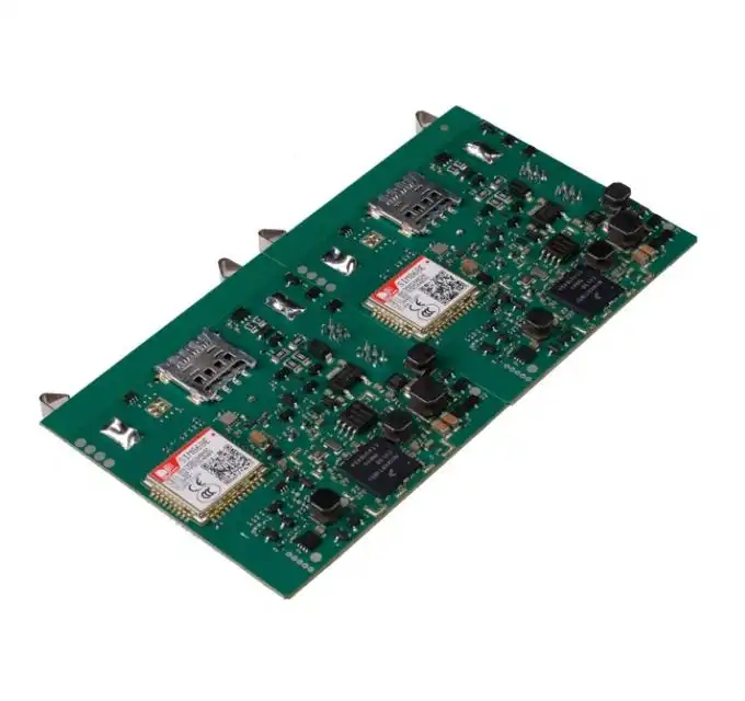
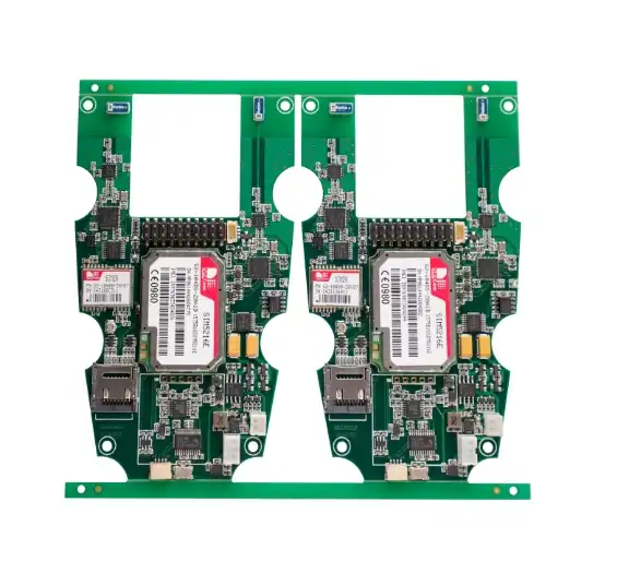
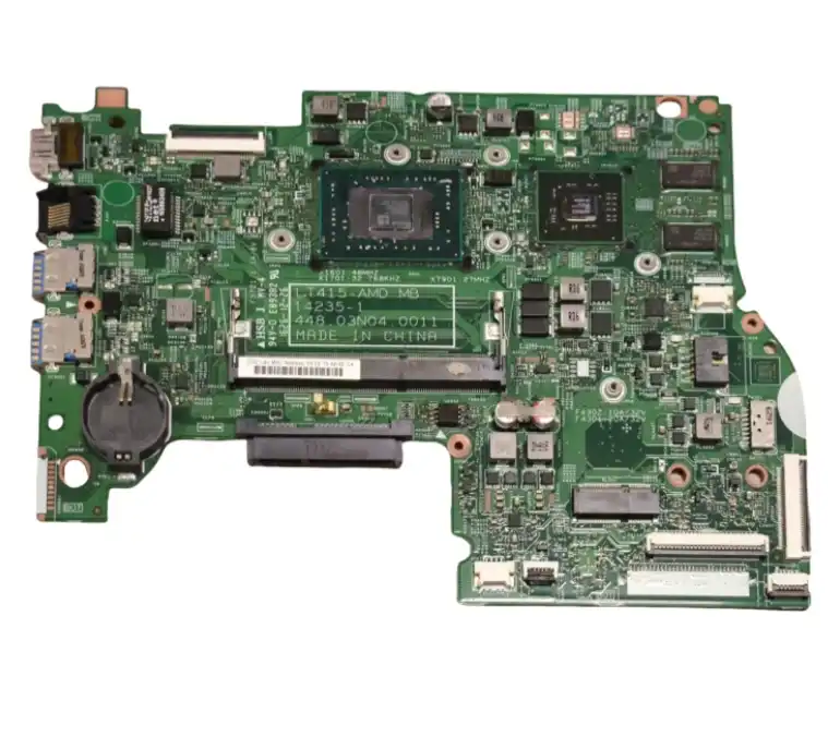
PCBA BGA Assembly represents a significant advancement in printed circuit board assembly techniques. This process involves attaching BGA components to PCBs, utilizing an array of solder balls on the underside of the package for electrical and mechanical connections. The technology has gained prominence due to its ability to accommodate high pin counts in a compact form factor, making it indispensable for high-density designs.
The Fundamentals of BGA Technology
BGA packages are characterized by their grid-like array of solder balls on the bottom surface. These balls serve as connectors between the integrated circuit and the PCB. Unlike traditional through-hole or surface-mount technologies, BGAs allow for a higher number of interconnections in a smaller area. This design enables better electrical performance by reducing lead lengths and minimizing signal distortions.
Applications Across Various Industries
The versatility of PCBA BGA Assembly has led to its widespread adoption across multiple sectors:
- Telecommunications: BGA components are essential in creating compact, high-performance networking equipment and mobile devices.
- Aerospace and Defense: The reliability and durability of BGA assemblies make them suitable for mission-critical systems in harsh environments.
- Consumer Electronics: From smartphones to gaming consoles, BGA technology enables the development of slim, feature-rich devices.
- Automotive Electronics: Advanced driver assistance systems (ADAS) and infotainment units benefit from the space-saving and performance advantages of BGA assemblies.
Advantages of BGA in High-Density Designs
The adoption of PCBA BGA Assembly in high-density designs offers several key benefits:
- Increased Functionality: The ability to pack more components into a smaller area allows for enhanced device capabilities.
- Improved Thermal Management: The larger surface area of BGA packages facilitates better heat dissipation, crucial for high-performance applications.
- Enhanced Signal Integrity: Shorter interconnect lengths reduce signal degradation and improve overall system performance.
- Flexibility in Design: BGA packages offer designers greater freedom in component placement and routing, optimizing PCB layouts.
The Technical Challenges and Solutions in PCBA BGA Assembly
While PCBA BGA Assembly offers numerous advantages, it also presents unique challenges that require sophisticated solutions. Understanding these challenges and implementing effective strategies is crucial for successful high-density PCB designs.
Precision Placement and Alignment
One of the primary challenges in BGA assembly is achieving precise component placement. The dense array of solder balls requires exact alignment with the corresponding pads on the PCB. Even slight misalignments can lead to connection failures or short circuits. To address this, advanced pick-and-place machines with high-precision optical alignment systems are employed. These machines use sophisticated vision systems and algorithms to ensure accurate positioning of BGA components.
Reflow Process Control
The reflow soldering process for BGA components is more complex than traditional surface-mount technologies. It requires careful control of temperature profiles to ensure proper solder ball melting and formation. Uneven heating can lead to issues such as tombstoning or solder bridging. To mitigate these risks, specialized reflow ovens with multiple heating zones and precise temperature control are used. Additionally, nitrogen atmosphere reflow systems can be employed to improve solder wetting and reduce oxidation.
Inspection and Quality Assurance
Inspecting BGA connections poses a unique challenge due to their hidden nature beneath the component. Traditional visual inspection methods are insufficient. To ensure quality, manufacturers employ advanced inspection techniques:
- X-ray Inspection: This non-destructive method allows visualization of solder joints, detecting issues like voids, insufficient solder, or bridging.
- Automated Optical Inspection (AOI): While limited in inspecting hidden connections, AOI systems can check for proper component placement and external solder joint quality.
- In-Circuit Testing (ICT): This electrical testing method verifies the functionality of the assembled PCB, including BGA connections.

Rework and Repair Considerations
Reworking BGA components requires specialized equipment and expertise. The process involves carefully removing the faulty component without damaging the PCB, preparing the site, and precisely placing and reflowing a new component. Advanced rework stations with localized heating and precision placement capabilities are essential for successful BGA rework operations.
Future Trends and Innovations in PCBA BGA Assembly
As technology continues to evolve, PCBA BGA Assembly is poised for further advancements. These innovations will play a crucial role in shaping the future of high-density electronic designs.
Miniaturization and Higher Density
The trend towards miniaturization shows no signs of slowing down. Future BGA packages are expected to feature even finer pitch sizes, allowing for higher component density. This evolution will enable the creation of more compact and powerful devices across various industries. However, it will also present new challenges in terms of assembly precision and thermal management.
Advanced Materials and Processes
Innovation in materials science is driving improvements in BGA technology. New solder alloys with enhanced thermal and electrical properties are being developed to meet the demands of high-performance applications. Additionally, advancements in underfill materials and application techniques are improving the reliability and longevity of BGA assemblies, particularly in harsh environments.
Integration of Artificial Intelligence
Artificial Intelligence (AI) is set to revolutionize PCBA BGA Assembly processes. AI-powered systems can optimize component placement, predict potential assembly issues, and enhance quality control processes. Machine learning algorithms can analyze vast amounts of production data to continuously improve assembly parameters and reduce defects.
Environmental Considerations
As sustainability becomes increasingly important, the electronics industry is focusing on eco-friendly BGA assembly processes. This includes the development of lead-free solder formulations, energy-efficient assembly equipment, and improved recycling techniques for BGA components. These efforts aim to reduce the environmental impact of electronic manufacturing while maintaining high performance standards.
3D Packaging Technologies
The future of BGA technology may lie in 3D packaging solutions. Stacked die configurations and through-silicon vias (TSVs) are emerging as potential successors to traditional BGA packages. These technologies promise even higher levels of integration and performance, opening new possibilities for high-density designs in applications such as artificial intelligence, high-performance computing, and advanced mobile devices.
Conclusion
PCBA BGA Assembly has become an indispensable technology in the realm of high-density electronic designs. Its ability to maximize component density while maintaining high performance and reliability has made it a cornerstone of modern electronics manufacturing. As we look to the future, continued innovations in BGA technology will undoubtedly play a crucial role in shaping the next generation of compact, powerful, and efficient electronic devices.
The challenges associated with BGA assembly, from precise placement to complex inspection requirements, have driven advancements in manufacturing processes and equipment. These developments have not only improved the quality and reliability of BGA assemblies but have also paved the way for even more sophisticated high-density designs.
As the electronics industry continues to evolve, embracing trends such as miniaturization, AI integration, and sustainable manufacturing, PCBA BGA Assembly will remain at the forefront of innovation. Its versatility and adaptability make it well-positioned to meet the demands of emerging technologies and applications across various sectors.
For manufacturers and designers alike, staying abreast of the latest developments in PCBA BGA Assembly technology is crucial. By leveraging these advancements, they can create cutting-edge products that push the boundaries of what's possible in electronic design, ultimately driving progress in industries ranging from consumer electronics to aerospace and beyond.
FAQ
What are the main advantages of using BGA components in PCB assembly?
BGA components offer higher pin counts in a smaller area, improved thermal performance, better electrical characteristics, and enhanced reliability in high-density designs.
How does PCBA BGA Assembly contribute to device miniaturization?
BGA technology allows for more components to be packed into a smaller space, enabling the creation of compact yet powerful electronic devices.
What are the key challenges in PCBA BGA Assembly?
The main challenges include precise component placement, controlling the reflow process, inspecting hidden solder joints, and performing rework when necessary.
How is quality control ensured in BGA assembly?
Quality control in BGA assembly typically involves X-ray inspection, automated optical inspection (AOI), and in-circuit testing (ICT) to ensure proper connections and functionality.
Expert PCBA BGA Assembly Services for High-Density Designs | Ring PCB
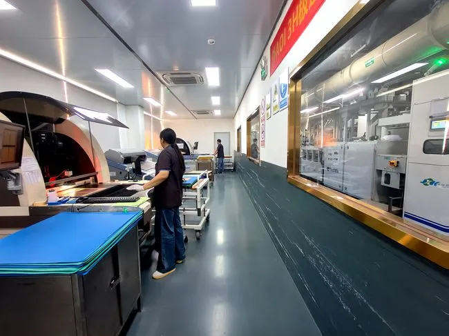
At Ring PCB, we specialize in advanced PCBA BGA Assembly for high-density designs. Our state-of-the-art facility is equipped with precision equipment for accurate component placement and reflow control. We offer comprehensive turnkey solutions, from PCB fabrication to final assembly and testing. Our expert team ensures optimal performance and reliability in your high-density designs. Experience the difference with our ISO9001 and IATF16949 certified processes. Contact us at [email protected] for your next project.
References
1. Johnson, R. W., et al. (2019). "The Changing Automotive Landscape: High-Density Packaging in ADAS Applications." IEEE Transactions on Electronics Packaging Manufacturing, 42(3), 182-195.
2. Zhang, L., & Liu, J. (2020). "Advances in BGA Assembly Techniques for High-Reliability Electronics." Journal of Manufacturing Science and Engineering, 142(8), 081001.
3. Pecht, M., & Gu, J. (2018). "Physics-of-Failure-Based Prognostics for Electronic Products." Transactions on Reliability, 58(3), 475-487.
4. Lee, Y. C., & Chen, W. T. (2021). "Design for Manufacturing and Assembly in BGA-Based High-Density PCBs." International Journal of Advanced Manufacturing Technology, 112(5), 1523-1537.
5. Lau, J. H., & Pao, Y. H. (2017). "Solder Joint Reliability of BGA, CSP, Flip Chip, and Fine Pitch SMT Assemblies." McGraw-Hill Professional Publishing.


