The PCB Assembly Process: From Design to Completion
Design and Preparation
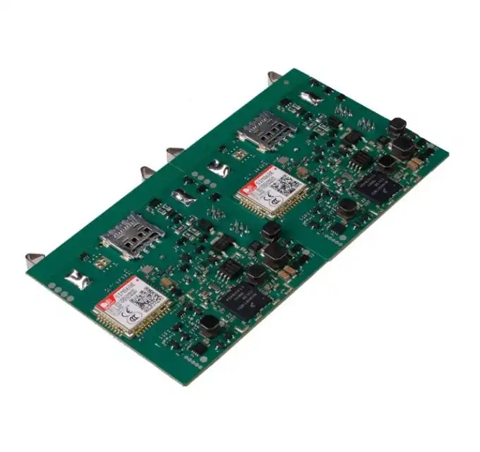
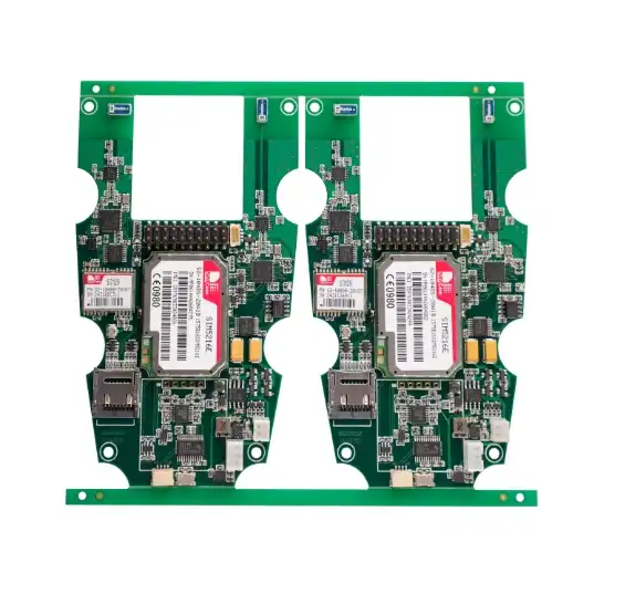
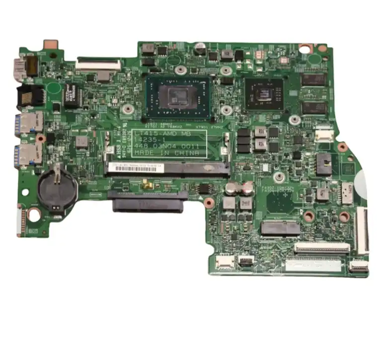
The PCB Assembly process begins long before any components are placed on the board. It starts with a meticulous design phase where engineers create a schematic of the circuit and translate it into a PCB layout. This layout serves as a blueprint for the entire assembly process, dictating where each component will be placed and how they will be connected.
Once the design is finalized, the bare PCB is manufactured. This involves creating the copper traces that will form the electrical connections between components. The PCB may have multiple layers, depending on the complexity of the circuit, with each layer serving a specific purpose in the overall design.
Preparation also includes the creation of a bill of materials (BOM), which lists all the components needed for the assembly. These components are then sourced and prepared for the assembly line. Quality control at this stage is crucial to ensure that all components meet the required specifications and are compatible with the PCB design.
Component Placement
The next stage in PCB Assembly is component placement. This is typically done using advanced pick-and-place machines that can accurately position hundreds of components per minute. These machines use computer vision systems and precise robotic arms to pick up components from reels or trays and place them in their designated positions on the PCB.
For surface mount components, a solder paste is first applied to the PCB using a stencil. This paste acts as both an adhesive to hold the components in place and as the material that will form the final solder joint. The pick-and-place machine then places the components onto these pads of solder paste.
Larger components or those that require through-hole mounting are often placed manually by skilled technicians. These components have leads that pass through holes in the PCB and are soldered on the opposite side.
Soldering and Reflow
After component placement, the PCB undergoes a soldering process to permanently attach the components and create electrical connections. For surface mount components, this is typically done through a reflow soldering process. The PCB is passed through a reflow oven where the temperature is carefully controlled to melt the solder paste, creating solid solder joints between the components and the PCB.
For through-hole components, wave soldering or selective soldering techniques are often used. In wave soldering, the PCB is passed over a wave of molten solder, which adheres to the exposed metal surfaces, forming solder joints. Selective soldering allows for more precise control and is often used for boards that have a mix of surface mount and through-hole components.
Inspection and Testing
Quality control is a critical aspect of PCB Assembly. After soldering, the boards undergo rigorous inspection and testing to ensure all components are correctly placed and functioning as intended. This often includes:
- Automated Optical Inspection (AOI): High-resolution cameras inspect the board for defects such as misaligned components or solder bridges.
- X-ray Inspection: Used to check solder joints that are not visible from the surface, particularly for ball grid array (BGA) components.
- In-Circuit Testing (ICT): Electrical tests to verify the functionality of individual components on the board.
- Functional Testing: The assembled PCB is tested to ensure it performs its intended functions correctly.
Any defects identified during these stages are either repaired or, if the defects are severe, the board may be scrapped and recycled.
Advanced Techniques in Modern PCB Assembly
Surface Mount Technology (SMT)
Surface Mount Technology has revolutionized PCB Assembly, allowing for much smaller and more densely packed circuits. SMT components are designed to be mounted directly onto the surface of the PCB, rather than having leads that pass through holes. This allows for components to be placed on both sides of the board, significantly increasing the circuit density.
The SMT process typically involves the following steps:
- Solder Paste Application: A precise amount of solder paste is applied to the PCB using a stencil.
- Component Placement: SMT pick-and-place machines rapidly and accurately position components onto the board.
- Reflow Soldering: The board is heated in a controlled environment to melt the solder paste and form permanent connections.
SMT allows for the use of very small components, such as 01005 resistors and capacitors, which are barely visible to the naked eye. This technology has been crucial in the development of compact electronic devices like smartphones and wearables.
Ball Grid Array (BGA) Assembly
Ball Grid Array is an advanced packaging technology used for integrated circuits with high pin counts. In BGA assembly, the component has an array of solder balls on its underside, which correspond to pads on the PCB. The assembly process for BGAs requires precise alignment and controlled reflow soldering.
BGA assembly offers several advantages:
- Higher Connection Density: BGAs can have hundreds of connections in a small area.
- Improved Electrical Performance: Shorter connection paths reduce signal degradation.
- Better Heat Dissipation: The large number of solder balls can help conduct heat away from the chip.
However, BGA assembly also presents challenges, particularly in inspection and rework. X-ray inspection is often necessary to verify the integrity of solder joints hidden beneath the component.
Flexible and Rigid-Flex PCB Assembly
As electronic devices become more compact and versatile, the demand for flexible and rigid-flex PCBs has increased. These types of PCBs present unique challenges in the assembly process:
- Material Handling: Flexible PCBs require careful handling to prevent damage or distortion during assembly.
- Component Placement: Specialized equipment may be needed to place components on flexible substrates accurately.
- Soldering: The thermal sensitivity of flexible materials requires precise control during soldering processes.
Rigid-flex PCBs, which combine rigid and flexible sections, require even more sophisticated assembly techniques. These boards often need to be assembled in stages, with careful attention paid to protecting flexible areas during the assembly of rigid sections.
Quality Control and Future Trends in PCB Assembly
Advanced Inspection Techniques
Quality control in PCB Assembly has evolved significantly with the introduction of advanced inspection technologies:
- 3D Automated Optical Inspection (AOI): This technology uses multiple cameras to create a three-dimensional image of the PCB, allowing for more accurate detection of defects such as insufficient solder or component tilt.
- Computed Tomography (CT) Scanning: Similar to medical CT scans, this technology can provide detailed 3D images of the entire PCB, including internal layers and hidden solder joints.
- Thermal Imaging: Used to detect potential issues related to power distribution and heat dissipation on the assembled PCB.
These advanced inspection techniques help ensure the reliability and quality of assembled PCBs, particularly for high-stakes applications in aerospace, medical devices, and automotive electronics.
Industry 4.0 and Smart Manufacturing
The concept of Industry 4.0, or the fourth industrial revolution, is making significant impacts on PCB Assembly. Smart manufacturing techniques are being increasingly adopted, including:
- IoT-enabled Equipment: Assembly machines connected to the Internet of Things (IoT) can provide real-time data on their performance and maintenance needs.
- Big Data Analytics: Large-scale data collection and analysis are being used to optimize assembly processes and predict potential issues before they occur.
- Artificial Intelligence: AI is being applied to various aspects of PCB Assembly, from optimizing component placement to enhancing quality control processes.
These technologies are driving towards more efficient, flexible, and higher-quality PCB Assembly processes.
Environmental Considerations
As global awareness of environmental issues grows, the PCB Assembly industry is also focusing on sustainability:
- Lead-free Soldering: The shift towards lead-free solders, driven by regulations like RoHS, continues to evolve with new alloy formulations.
- Energy Efficiency: Assembly equipment is being designed to be more energy-efficient, reducing the carbon footprint of the manufacturing process.
- Waste Reduction: Advanced planning and simulation tools are being used to optimize material usage and reduce waste in the assembly process.
- Recyclability: There's an increasing focus on designing PCBs and choosing components with end-of-life recyclability in mind.
These environmental considerations are not just about compliance with regulations, but also about meeting the growing demand from consumers for more sustainable electronic products.
Conclusion
PCB Assembly is a complex and evolving field that combines precision engineering with advanced manufacturing techniques. From the initial design to the final quality control, each step in the process is crucial for creating reliable and high-performing electronic devices. As technology continues to advance, PCB Assembly techniques are also evolving, embracing new technologies like AI and IoT to improve efficiency and quality.
For businesses looking for a reliable PCB Assembly supplier or manufacturer, it's crucial to choose a partner that not only has the technical capabilities but also stays abreast of the latest trends and technologies in the field. A skilled PCB Assembly manufacturer can significantly impact the quality, performance, and cost-effectiveness of your electronic products.
FAQ
What is the difference between PCB fabrication and PCB Assembly?
PCB fabrication involves creating the bare circuit board with copper traces, while PCB Assembly is the process of attaching components to this board.
How long does the PCB Assembly process typically take?
The duration varies depending on the complexity and volume of the boards, but it can range from a few hours for simple boards to several days for complex, high-volume productions.
What are the most common defects in PCB Assembly?
Common defects include solder bridges, component misalignment, insufficient solder, and tombstoning (where a component stands on one end).
Expert PCB Assembly Services | Ring PCB
At Ring PCB, we offer state-of-the-art PCB Assembly services tailored to meet the diverse needs of various industries. Our advanced engineering capabilities, including high-density stack-up and smart manufacturing, ensure precision and quality in every project. With our integrated PCBA services and rigorous quality control measures, we deliver reliable, high-performance PCBs. Our self-owned factory and full supply chain control guarantee efficiency and consistency. For expert PCB Assembly solutions, contact us at [email protected].
References
1. Smith, J. (2022). "Advanced Techniques in Modern PCB Assembly". Journal of Electronics Manufacturing, 15(3), 123-145.
2. Johnson, A. & Brown, B. (2021). "Quality Control Innovations in PCB Assembly". IEEE Transactions on Electronics Packaging Manufacturing, 44(2), 78-92.
3. Lee, C. (2023). "Environmental Considerations in PCB Manufacturing and Assembly". Sustainable Electronics Review, 8(1), 45-60.
4. Wilson, R. (2022). "Industry 4.0 and Its Impact on PCB Assembly Processes". Smart Manufacturing Quarterly, 12(4), 201-215.
5. Garcia, M. & Thompson, K. (2023). "The Future of Flexible and Rigid-Flex PCB Assembly". Flexible Electronics Journal, 7(2), 112-128.


