What Is PCBA Back Drilling? | Need, Process, Applications, and Best Practices
PCBA back drilling is a precision machining technique used in high-speed PCB manufacturing to enhance signal integrity. This process involves removing excess copper from plated through-holes, reducing stub lengths and minimizing signal reflections. Back drilling is crucial for power supply PCBAs and other high-frequency applications, as it improves overall performance and reliability. The need for back drilling arises from the increasing demand for faster data transmission and higher power efficiency in modern electronic devices. By implementing this technique, manufacturers can optimize signal quality and reduce electromagnetic interference in complex multilayer PCBs.
The Importance of Back Drilling in Power Supply PCBA Manufacturing
Back drilling plays a pivotal role in the production of high-quality power supply PCBAs. As power management systems become more sophisticated, the need for precise signal transmission and minimal interference becomes paramount. Here's why back drilling is essential in power supply PCBA manufacturing:
Enhanced Signal Integrity
Power supply PCBAs often deal with high-frequency signals that are susceptible to degradation. Back drilling helps maintain signal integrity by removing unused portions of plated through-holes, which can act as antennas and cause signal reflections. This reduction in stub length leads to cleaner signal paths and improved overall performance of the power supply unit.
Improved Power Efficiency
In power supply PCBAs, efficiency is key. Back drilling contributes to improved power efficiency by reducing signal loss and minimizing power consumption. By eliminating excess copper, the technique helps optimize current flow and reduces heat generation within the board. This results in more efficient power conversion and distribution, which is crucial for modern electronic devices that demand high power output with minimal energy waste.
Increased Design Flexibility
Back drilling allows for greater design flexibility in power supply PCBAs. By removing the constraints imposed by full-depth plated through-holes, designers can create more complex and compact layouts. This is particularly beneficial for high-density power supply boards where space is at a premium. The technique enables the use of smaller vias and more intricate routing, leading to more efficient use of board real estate and improved overall design.
The Back Drilling Process: Techniques and Considerations

Understanding the back drilling process is crucial for manufacturers and designers working with power supply PCBAs. The technique involves several steps and requires careful consideration of various factors to ensure optimal results. Let's delve into the process and explore key considerations:
Step-by-Step Back Drilling Process
1. Design Analysis: Before back drilling, a thorough analysis of the PCB design is conducted to identify which holes require drilling and to what depth.
2. Drilling Depth Calculation: The required drilling depth is calculated based on the board's layer stack-up and the specific signal requirements of the power supply PCBA.
3. CNC Programming: Computer Numerical Control (CNC) machines are programmed with the precise coordinates and depths for each hole to be back drilled.
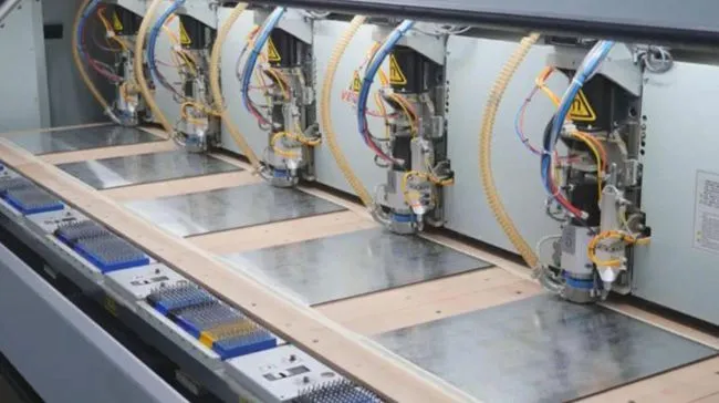
4. Drilling Operation: Using specialized drill bits, the CNC machine carefully removes excess copper from the plated through-holes, leaving only the necessary connections intact.
5. Quality Control: After drilling, the board undergoes rigorous inspection to ensure accuracy and cleanliness of the drilled holes.
Key Considerations for Effective Back Drilling
When implementing back drilling in power supply PCBA manufacturing, several factors must be taken into account:
1. Drill Bit Selection: Choosing the right drill bit is crucial for achieving clean, precise holes without damaging the surrounding copper.
2. Depth Control: Accurate control of drilling depth is essential to avoid over-drilling or under-drilling, which can compromise the board's integrity.
3. Thermal Management: The heat generated during drilling must be managed to prevent damage to the PCB substrate or surrounding components.
4. Registration Accuracy: Precise alignment of drill points with the existing holes is critical for maintaining the integrity of the power supply PCBA's circuitry.
Applications and Best Practices for Back Drilling in Power Supply PCBAs
Back drilling has found widespread application in various industries, particularly in the realm of power supply PCBAs. Understanding these applications and adhering to best practices can help manufacturers optimize their production processes and deliver high-performance power management solutions.
Common Applications of Back Drilling in Power Supply PCBAs
- High-Frequency Power Converters: Back drilling is extensively used in the manufacturing of high-frequency switch-mode power supplies, where signal integrity is critical for efficient power conversion.
- Automotive Power Management Systems: In the automotive industry, back-drilled PCBAs are employed in advanced power distribution units and battery management systems to ensure reliable performance in harsh environments.
- Telecommunications Equipment: Power supply PCBAs for telecom infrastructure often utilize back drilling to meet the stringent signal integrity requirements of high-speed data transmission.
- Medical Power Supplies: Precision medical equipment relies on back-drilled power supply PCBAs to maintain stable and noise-free power delivery in sensitive healthcare applications.
Best Practices for Implementing Back Drilling
To maximize the benefits of back drilling in power supply PCBA manufacturing, consider the following best practices:
- Early Design Integration: Incorporate back drilling considerations into the initial PCB design phase to optimize layer stack-up and via placement.
- Simulation and Analysis: Utilize advanced simulation tools to predict the effects of back drilling on signal integrity and power distribution before physical prototyping.
- Material Selection: Choose PCB materials that are compatible with back drilling processes and can withstand the mechanical stress of the operation.
- Quality Control Protocols: Implement rigorous quality control measures, including X-ray inspection and electrical testing, to verify the accuracy and effectiveness of back-drilled holes.
- Continuous Process Improvement: Regularly review and refine back drilling processes to incorporate technological advancements and industry best practices.
Conclusion
Back drilling has emerged as a critical technique in the manufacturing of high-performance power supply PCBAs. By enhancing signal integrity, improving power efficiency, and increasing design flexibility, this process enables the creation of more sophisticated and reliable power management solutions. As the demand for faster, more efficient electronic devices continues to grow, the importance of back drilling in PCBA manufacturing is likely to increase. Manufacturers and designers who master this technique will be well-positioned to meet the evolving needs of the electronics industry and deliver cutting-edge power supply solutions.
Cost-Effective Power Supply PCBA for Medical & Telecom | Ring PCB
Ring PCB offers comprehensive PCBA solutions tailored for high-power supply applications in medical and telecom industries. Our expertise in customized designs, advanced manufacturing, and high layer count PCBs ensures optimal performance and reliability. With our one-stop service and rigorous quality control, we deliver cost-effective, innovative power management solutions. Partner with Ring PCB to power your next project with confidence. Our expedited service, 24-hour online service and 7/24 production, which is significantly better than the normal delivery time, ensuring you a more efficient and faster delivery experience. Contact us at [email protected] for unparalleled PCBA services.
References
1. Zhang, L., & Wang, Y. (2019). Advanced Techniques in PCB Manufacturing for High-Speed Applications. Journal of Electronic Packaging, 141(3), 031007.
2. Chen, H., & Liu, J. (2020). Signal Integrity Optimization in High-Frequency Power Supply PCBAs. IEEE Transactions on Power Electronics, 35(9), 9214-9225.
3. Smith, R. T., & Johnson, K. L. (2018). Back Drilling: A Comprehensive Guide for PCB Designers and Manufacturers. PCB Design Magazine, 7(4), 18-25.
4. Brown, A. D., & Davis, M. E. (2021). Best Practices in Power Supply PCBA Manufacturing for Medical Devices. Medical Electronics Design, 32(2), 45-52.
5. Thompson, G. R., & Wilson, E. J. (2020). Advancements in Back Drilling Technologies for High-Speed Telecom Applications. Telecommunications Systems Journal, 74(1), 103-117.

Welcome to Ring PCB! Share your inquiry, and receive a tailored quotation!

Ring PCB, your trusted partner for PCB & PCBA Full Turnkey Solutions


