What is the difference between PCB assembly and PCB manufacturing?
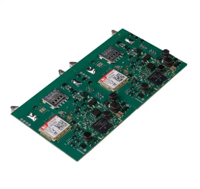
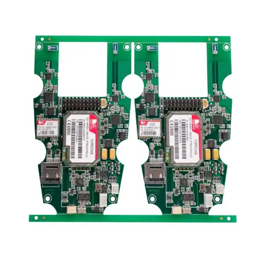
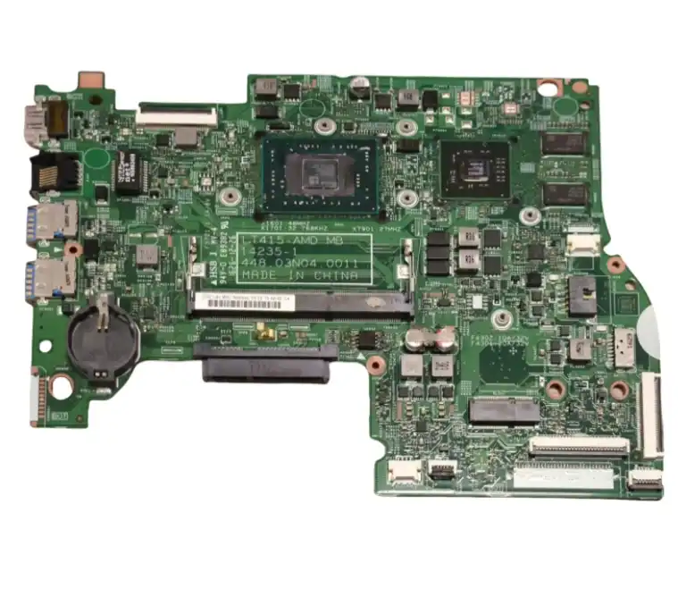
PCB manufacturing and PCB assembly are two distinct yet interconnected processes in the creation of electronic devices. PCB manufacturing involves the production of bare printed circuit boards, which serve as the foundation for electronic components. This process includes designing the circuit layout, etching copper traces, and applying solder mask and silkscreen. On the other hand, PCB assembly (PCBA) is the process of populating these bare boards with electronic components such as resistors, capacitors, and integrated circuits. PCBA involves soldering components onto the board, often using techniques like surface-mount technology (SMT) or through-hole assembly. While PCB manufacturing creates the physical board, PCB assembly transforms it into a functional electronic circuit.
The Intricacies of PCB Manufacturing: From Design to Bare Board
Design and Layout: The Blueprint of PCB Manufacturing
PCB manufacturing begins with the crucial step of design and layout. Engineers use specialized software to create a schematic diagram that represents the electronic circuit. This schematic is then translated into a physical layout, determining the placement of components and routing of copper traces. The layout must consider factors such as signal integrity, thermal management, and electromagnetic compatibility.
During this phase, designers must adhere to design rules that ensure manufacturability and reliability. These rules dictate minimum trace widths, spacing between components, and other critical parameters. The complexity of modern electronics often necessitates multi-layer PCBs, where the circuit is distributed across several layers of copper sandwiched between insulating materials.
Material Selection: The Foundation of PCB Quality
The choice of materials in PCB manufacturing significantly impacts the board's performance and durability. The base material, typically a fiberglass-reinforced epoxy laminate known as FR-4, provides mechanical strength and electrical insulation. For high-frequency applications, specialized materials with low dielectric constants may be used to minimize signal loss.
Copper foil, the conductive layer where circuit traces are etched, comes in various thicknesses. Heavier copper weights are used for high-current applications, while thinner foils allow for finer trace widths in dense layouts. The selection of copper thickness must balance electrical requirements with manufacturing constraints.
Fabrication Process: Bringing the PCB to Life
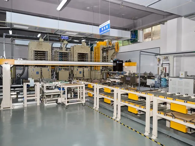
The actual fabrication of the PCB involves a series of chemical and mechanical processes. It begins with imaging the circuit pattern onto the copper-clad board using photoresist and UV light. The exposed copper is then etched away, leaving behind the desired circuit traces. For multi-layer boards, this process is repeated for each layer, with insulating layers and copper foils bonded together in a high-pressure lamination process.
After etching, the boards undergo drilling to create holes for through-hole components and vias that connect different layers. These holes are then plated with copper to ensure electrical connectivity. The final steps include applying solder mask to protect the copper traces and silkscreen for component markings and identifiers.
PCB Assembly: Transforming Bare Boards into Functional Circuits
Component Procurement: Sourcing the Building Blocks
PCB assembly begins with the procurement of electronic components specified in the bill of materials (BOM). This process requires careful attention to component specifications, availability, and cost. Sourcing components from reliable suppliers is crucial to ensure quality and avoid counterfeit parts that could compromise the final product's reliability.
In today's global supply chain, component procurement can be complex, especially for specialized or high-demand parts. Many PCB assembly services offer component sourcing as part of their turnkey solutions, leveraging their industry relationships to secure the necessary parts efficiently and cost-effectively.
Surface Mount Technology (SMT): Precision at Scale
Surface Mount Technology (SMT) is the predominant method used in PCB assembly for attaching components to the board. This process begins with applying solder paste to the board using a stencil. The paste is precisely deposited on the copper pads where components will be placed.
Next, a pick-and-place machine accurately positions surface mount components onto the board. These machines can place thousands of components per hour with high precision. The populated board then passes through a reflow oven, where the solder paste melts and forms solid electrical connections as it cools.
SMT allows for higher component density and smaller form factors compared to through-hole assembly, making it ideal for modern, compact electronic devices. However, it requires careful control of temperature profiles and component alignment to ensure reliable connections.
Through-Hole Assembly: Strength and Reliability
While SMT dominates modern PCB assembly, through-hole assembly still plays a vital role, especially for components that require stronger mechanical connections or need to handle high power or heat. In through-hole assembly, component leads are inserted through holes in the PCB and soldered on the opposite side.
This process can be done manually for small production runs or prototypes, or automated using machines for larger volumes. Wave soldering is a common technique for through-hole assembly, where the bottom of the board passes over a wave of molten solder, forming connections for all through-hole components simultaneously.
Through-hole assembly offers advantages in terms of mechanical strength and ease of rework, making it suitable for certain applications like aerospace or industrial equipment where reliability under harsh conditions is paramount.
Quality Assurance in PCB Manufacturing and Assembly
Inspection Techniques: Ensuring Perfection
Quality assurance is critical in both PCB manufacturing and assembly to ensure the reliability and functionality of the final product. In PCB manufacturing, inspection techniques such as Automated Optical Inspection (AOI) and X-ray inspection are used to detect defects in the bare board, including incorrect trace widths, missing vias, or copper shorts.
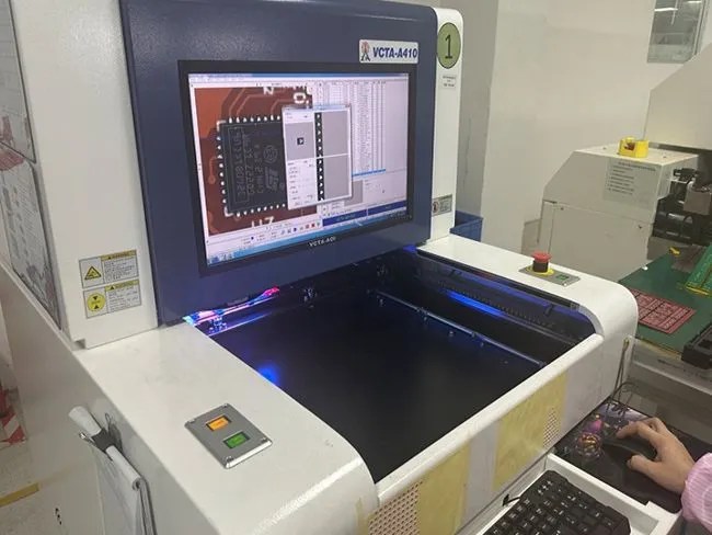
During PCB assembly, these inspection methods are augmented with additional techniques. AOI systems check for correct component placement, orientation, and solder joint quality. X-ray inspection is particularly useful for examining hidden solder joints in ball grid array (BGA) components or multi-layer boards.
Functional Testing: Validating Performance
Beyond visual inspection, functional testing is crucial to verify that the assembled PCB performs as intended. This can range from simple continuity tests to complex automated test equipment that simulates the PCB's operating conditions. In-Circuit Testing (ICT) uses a bed-of-nails fixture to make contact with test points on the board, allowing for rapid testing of individual components and connections.
For more complex assemblies, functional testing may involve powering up the board and running diagnostic software to ensure all systems are operating correctly. This level of testing is essential for detecting issues that may not be visible through inspection alone, such as timing problems or component interactions.
Environmental and Reliability Testing
To ensure that PCBs can withstand their intended operating conditions, manufacturers often conduct environmental and reliability testing. This can include thermal cycling to simulate temperature fluctuations, humidity testing to check for moisture resistance, and vibration testing to ensure mechanical stability.
For industries with stringent reliability requirements, such as automotive or aerospace, additional tests like highly accelerated life testing (HALT) or highly accelerated stress screening (HASS) may be employed. These tests push the PCB assembly to its limits, helping to identify potential failure modes and improve overall product reliability.
Conclusion
Understanding the distinction between PCB manufacturing and PCB assembly is crucial for anyone involved in the electronics industry. While PCB manufacturing focuses on creating the bare circuit board, PCB assembly brings that board to life by populating it with components. Both processes require precision, expertise, and attention to detail to produce high-quality electronic devices.
As technology continues to advance, the challenges and opportunities in both PCB manufacturing and assembly evolve. From the increasing density of components to the adoption of new materials and technologies, the field remains dynamic and innovative. Whether you're designing a simple circuit or a complex electronic system, a deep understanding of these processes can help you make informed decisions and optimize your product development.
From bare board to functional product — we do both | Ring PCB
Ring PCB Technology Co., Limited is your trusted PCB Manufacturing Partner since 2008, offering comprehensive one-stop services for PCB and PCBA. With 17 years of excellence, we deliver innovative, reliable, and cost-effective solutions for diverse industries. Our state-of-the-art Shenzhen factory, equipped with advanced SMT lines and rigorous quality control measures, ensures top-notch products. From customized designs to high layer count PCBs, we provide tailored solutions to meet your exact requirements. Partner with Ring PCB for unparalleled expertise in PCB manufacturing and assembly.
Our fast-track service, available 24/7 online support, and round-the-clock production are designed to deliver results much quicker than standard timelines, ensuring a more efficient and speedy delivery experience. For more information on PCB manufacturing and assembly services, or to discuss your specific project needs, don't hesitate to reach out to industry experts. Contact us at [email protected] to learn how we can support your electronic manufacturing needs.
References
1. Smith, J. (2022). "Advanced Printed Circuit Board Design and Manufacturing Techniques". IEEE Press.
2. Johnson, M. R. (2021). "PCB Assembly Processes: From Manual to Automated Solutions". Journal of Electronics Manufacturing, 15(2), 78-92.
3. Lee, S. H., & Park, Y. J. (2020). "Quality Assurance Methodologies in Modern PCB Manufacturing". International Journal of Quality Engineering and Technology, 8(4), 301-315.
4. Thompson, R. A. (2023). "The Evolution of Surface Mount Technology in PCB Assembly". Proceedings of the Annual Electronics Manufacturing Symposium, 112-125.
5. Chen, L., & Wang, Q. (2021). "Material Innovations in High-Performance PCB Manufacturing". Advanced Materials for Electronics, 7(3), 189-204.

Welcome to Ring PCB! Share your inquiry, and receive a tailored quotation!

Ring PCB, your trusted partner for PCB & PCBA Full Turnkey Solutions
