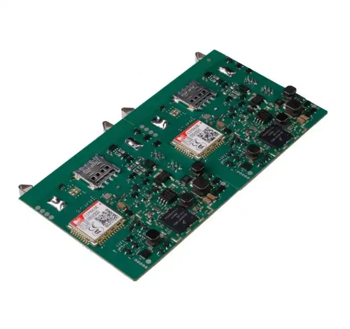
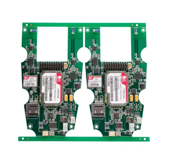
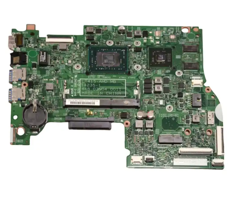
Common PCB Assembly Problems and How to Fix Them
Production schedules, product quality, and manufacturing costs may all be greatly impacted by PCB Assembly problems in the electronic industries. These issues, which range from solder flaws and component misalignment to heat damage and electrical malfunctions, need for methodical detection and focused fixes. Manufacturers may maintain consistent quality while lowering rework rates and production delays by comprehending the underlying reasons and putting established rectification techniques into practice. Reliable electronic products that satisfy exacting industry standards and customer expectations are ensured by rapidly resolving assembly difficulties, whether they include surface mount technology or through-hole components.
Understanding Common PCB Assembly Problems
The many obstacles that modern electronics manufacturing must overcome might raise production costs and jeopardize product dependability. There are several chances for assembly flaws to arise due to the complexity of today's circuit boards, miniaturization trends, and strict performance standards.
Solder Joint Defects and Their Origins
In production settings, solder joint difficulties are the most common assembly challenges. Cold solder junctions are weak connections that might break during testing or operation because there is not enough heat to properly metallurgize the link between components and pads. Excess paste may create short circuits or other functional problems by forming solder bridges, which are undesired electrical connections between neighboring pads.
Unbalanced solder paste application or uneven heating may cause one end of tiny passive components to rise away from the pad during reflow, a phenomenon known as tombstoning. With package sizes 0201 and 01005, which are often seen in mobile devices and small electronics, this condition becomes more troublesome.
Component Placement and Alignment Issues
Accurate component placement is essential for mechanical stability and dependable electrical connections. When working with fine-pitch packages like QFNs and BGAs, where assembly success depends on micron-level precision, placement accuracy becomes difficult. Placement quality is affected by environmental conditions, pick-and-place machine maintenance, and vision system calibration.
While X-Y offset produces stress concentrations that might cause early failure, rotational misalignment can hinder the creation of a good solder junction. Worn tooling, improper programming, or insufficient board support during assembly processes are often the causes of these problems.
Thermal and Mechanical Stress Problems
Damage caused by temperature happens at every stage of the manufacturing process, from handling components to final testing. Sensitive semiconductor devices continue to be at risk from electrostatic discharge, necessitating thorough ESD management procedures. Long-term dependability may be jeopardized by board warping during reflow, which might result in component displacement or unequal solder junctions in PCB Assembly.
In demanding applications like automotive electronics, the interplay between the thermal expansion coefficients of various materials creates stress that builds up throughout temperature cycling and may result in joint fatigue or component breakage.
Step-by-Step Solutions to Fix PCB Assembly Problems
Systematic procedures that integrate appropriate diagnostic technologies with tried-and-true corrective strategies are necessary to address assembly problems. Accurately identifying the issue and using the right instrument for each unique circumstance are essential to successful rehabilitation.
Diagnostic Tools and Inspection Methods
With the use of high-resolution imagery and complex algorithms, automated optical inspection systems provide thorough defect detection capabilities, detecting component corrosion, solder connection issues, and positioning mistakes. Although these systems are excellent at identifying obvious flaws, they could overlook obscure problems such internal component corrosion or voiding.
By exposing the interior solder joint structure, X-ray inspection makes it possible to assess the quality of through-hole fill, BGA connections, and void content, all of which have an impact on thermal performance. Both 2D and 3D imaging capabilities are available with modern X-ray equipment, giving precise images of intricate components without the need for harmful testing.
Through the identification of openings, shorts, other parametric faults that are invisible to the naked eye, in-circuit testing verifies electrical connection and component values. Bed-of-nails fixtures allow high-speed testing for volume manufacturing, while flying probe testers give flexibility for prototype and low-scale production.
Rework and Correction Techniques
Controlled heating is necessary for professional rework in order to prevent damage to nearby components or board substrates. When paired with the right flux application and thermal profiling, hot air stations with precise temperature control allow for the safe removal and replacement of components. Interchangeable-tip soldering irons can handle a variety of package kinds without sacrificing joint quality.
Solder bridge removal separates undesired connections by applying flux or desoldering braid and then applying regulated heating. Before solder solidifies, component readjustment requires precise placement via cautious heating and light pressure. A successful rework restores complete functionality while preserving board integrity.
Quality Verification After Repair
Inspection after rework guarantees that corrections are effective without creating new flaws. Electrical testing verifies functionality restoration, while visual inspection verifies correct component placement and solder connection appearance. For important applications, thermal cycling could be necessary to confirm joint reliability under stress.
Defect trend analysis and process improvement are made possible by documenting rework actions. By documenting defect types, underlying causes, and remediation techniques, institutional knowledge is developed that reduces the likelihood of reoccurring issues and enhances assembly quality overall.
Preventing PCB Assembly Defects: Design and Process Guidelines
By improving design techniques and streamlining production procedures, prevention tactics lower fault rates by addressing the underlying causes of problems rather than their symptoms. Design and manufacturing teams working together guarantees producibility in PCB Assembly while upholding performance standards.
Design for Manufacturing Principles
Yield rates are increased and assembly difficulties are reduced when DFM rules are used during layout design. While pad layouts maximize solder connection formation for certain package types, component spacing requirements take manufacturing tolerances and inspection access into account. Appropriate land patterns provide sufficient solder volume for dependable connections while accommodating placement precision constraints.
Copper balance to avoid uneven heating during reflow, component orientation to reduce thermal stress, and strategic via placement for heat dissipation are all examples of thermal management issues. Effective electrical verification is made possible by test point accessibility without sacrificing board density or signal integrity.
The following crucial DFM procedures have a big influence on assembly success:
• Component spacing optimization ensures adequate clearance for placement equipment while providing inspection access for quality verification processes
• Land pattern standardization follows IPC guidelines for consistent solder joint formation across different package types and manufacturing environments
• Thermal balancing techniques distribute copper evenly to prevent warping and ensure uniform heating during reflow operations
• Via management strategies optimize placement for thermal relief while maintaining signal integrity and manufacturing feasibility requirements
These DFM principles work together to create robust designs that withstand manufacturing variations while maintaining high assembly yields and long-term reliability.
Process Control and Optimization
Defect rates and joint formation are directly impacted by the quality of solder paste printing. Specific assembly criteria must be addressed via stencil design, paste selection, and printing settings. Frequent examination and cleaning of the stencil avoids aperture blockage, which results in either too much or too little paste deposition.
Optimizing the reflow profile guarantees correct solder connection creation without causing heat damage to substrates or components. The cooling rate, peak temperature, and time-above-liquidus factors need to be carefully balanced according to component specifications and board thermal mass. Consistency between manufacturing batches is confirmed by profile monitoring using thermocouples connected to representative assemblies.
Supplier Quality Management
Long-term dependability and assembly success rates are directly impacted by component quality. Protocols for incoming inspections confirm component specifications, package integrity, and handling of moisture-sensitive materials. Throughout the supply chain, supplier audits guarantee consistent quality systems and appropriate storage conditions.
Material traceability facilitates failure analysis investigations and allows for quick reaction to quality concerns. Documentation pertaining to certificates of conformity ensures that components adhere to environmental rules such as REACH and RoHS.
Advanced PCB Assembly Troubleshooting and Testing Techniques
Complex electronic assemblies require sophisticated diagnostic approaches that go beyond basic visual inspection and simple electrical testing. Modern troubleshooting combines multiple technologies to identify subtle defects that could cause field failures.
Comprehensive Electrical Testing Strategies
By using the built-in test capabilities of intricate digital devices, boundary scan testing allows for thorough connection verification without the need for physical probe access. This method works particularly well for high-density assemblies when probe accessibility issues make standard in-circuit testing unfeasible.
Functional testing finds integration problems that component-level testing may overlook by verifying whole system function under realistic circumstances. Custom test fixtures provide controlled stimulation and measurement capabilities while simulating operational settings in PCB Assembly. Protocols for software-based testing confirm communication interfaces and firmware functionality.
Thermal Analysis and Reliability Assessment
By revealing temperature distributions during operation, thermal imaging may uncover hot patches that can point to assembly flaws or design flaws. Comparative evaluation of questionable units and known-good assembly aids in identifying trouble spots for in-depth research.
Assemblies are exposed to higher temperatures and voltages during accelerated life testing, which also keeps an eye out for failure mechanisms or deterioration. Before volume manufacturing starts, this method finds possible areas for improvement and confirms long-term dependability estimates.
Specialized Diagnostic Equipment
By showing interior structure and detecting flaws like voiding, intermetallic development, or inadequate wetting, micro-sectioning offers thorough cross-sectional views of solder connections. For failure investigation and process validation investigations, this disruptive approach provides conclusive analysis.
Time-domain reflectometry detects impedance discontinuities that impact high-speed digital performance and quantifies signal integrity. For RF applications where precise control of electrical performance is necessary, network analyzers describe insertion loss and frequency responsiveness.
Our Expertise and Comprehensive PCB Assembly Solutions
Ring PCB Technology Co., Limited stands as your trusted manufacturing partner since 2008, delivering exceptional circuit board solutions across diverse industries. Our commitment to excellence spans 18 years of continuous innovation, quality improvement, and customer satisfaction in the competitive electronics manufacturing landscape.
State-of-the-Art Manufacturing Capabilities
Our 10,000 square meter facility is equipped with cutting-edge equipment for quality control and precise manufacture. Vacuum lamination technology creates dependable multilayer stackups, while LDI laser exposure technologies guarantee precise trace definition. Without the lead periods connected with conventional fixture-based testing techniques, flying probe testers provide thorough electrical verification.
Manufacturing capabilities range from simple single-layer boards to intricate 48-layer structures with buried and blind vias. Demanding applications in 5G infrastructure, medical devices, and automotive electronics, where performance needs continue to push technical frontiers, are supported by high-density designs with 3/3mil trace and spacing geometries.
Integrated Turnkey Services
Through strategic alliances and vertical integration, our all-inclusive service offering removes supply chain complexity. Complete turnkey solutions are produced by combining PCB manufacturing skills with knowledge of acquiring electronic components. With remarkable placement precision, SMT assembly services manage packages ranging from huge through-hole components to ultra-fine pitch devices.
By offering full product integration, including mechanical assembly, cable harnessing, and final system testing, box-building services go beyond board-level assembly. This all-encompassing strategy guarantees constant quality standards throughout the production process while lowering coordination complexity.
Quality Assurance and Certifications
Multiple international certifications demonstrate our commitment to quality excellence and regulatory compliance. ISO9001 quality management systems ensure consistent processes and continuous improvement initiatives. IATF16949 automotive certification validates our capability to meet stringent automotive industry requirements for quality and traceability.
Here are our key quality achievements that ensure superior assembly results:
• Triple quality assurance protocols combine AOI inspection, impedance testing, and thermal cycling validation to achieve defect rates below 0.2 percent
• Advanced inspection capabilities utilize X-ray systems and automated optical inspection for comprehensive defect detection across all assembly types
• 100% functional validation ensures every assembly meets specifications before shipment, eliminating costly field failures and customer disruptions
• IPC-6012 Class 3 compliance provides the highest reliability standards for mission-critical applications in aerospace, medical, and military sectors
These quality measures work synergistically to deliver assemblies that exceed customer expectations while maintaining competitive pricing and delivery schedules.
Conclusion
PCB assembly issues need thorough comprehension of the underlying reasons in addition to methodical corrective measures and effective preventative measures. Integrating sound design principles, efficient manufacturing procedures, and cutting-edge diagnostic tools throughout the production lifecycle are essential for success. In order to fulfill increasingly demanding performance criteria and obtain consistent outcomes, modern assembly difficulties need cooperation between design teams, production engineers, and quality specialists. In today's cutthroat electronics manufacturing industry, the basis for long-term quality improvement and customer satisfaction is provided by investments in suitable inspection equipment, process control systems, and operator training.
FAQ
Q1: What are the most common types of soldering defects in PCB assembly?
A: The most prevalent soldering defects include cold solder joints caused by insufficient heating, solder bridges creating unwanted electrical connections, and tombstoning where small components lift during reflow. Additionally, insufficient solder coverage, excessive voiding, and thermal damage represent significant quality concerns that require immediate attention and process adjustment.
Q2: How can manufacturers reduce rework rates while maintaining fast turnaround times?
A: Implementing comprehensive design for manufacturability reviews before production begins prevents many assembly issues. Optimizing solder paste printing parameters, maintaining consistent reflow profiles, and utilizing automated optical inspection for early defect detection significantly reduces rework requirements. Proper operator training and equipment maintenance also contribute to improved first-pass yields.
Q3: Which inspection methods provide the most comprehensive defect detection for complex assemblies?
A: Combining automated optical inspection with X-ray imaging offers the most thorough defect coverage. AOI systems excel at detecting visible placement and solder joint issues, while X-ray reveals hidden problems like BGA voiding and through-hole fill quality. In-circuit testing validates electrical connectivity, providing complete assembly verification when used together.
Q4: What design considerations help prevent assembly problems during manufacturing?
A: Optimizing component spacing for placement equipment clearance, following IPC land pattern guidelines, and implementing thermal balancing techniques prevent most assembly issues. Providing adequate test points for electrical verification and considering manufacturing tolerances during layout design significantly improves assembly success rates and reduces production delays.
Partner with Ring PCB for Superior Assembly Quality
Ring PCB delivers exceptional assembly solutions through advanced manufacturing capabilities and comprehensive quality assurance protocols. Our 48-layer multilayer circuit board technology, combined with ISO certifications and 24/7 production schedules, ensures superior results for demanding applications. As a trusted PCB assembly manufacturer, we provide competitive pricing while maintaining the highest quality standards through our experienced engineering team and state-of-the-art facilities. Contact our specialists at [email protected] to discuss your specific requirements and discover how our turnkey services can optimize your supply chain efficiency while reducing costs and delivery times.
References
1. Smith, J.R., and Williams, M.K. "Advanced Soldering Techniques for Modern PCB Assembly." Journal of Electronics Manufacturing, vol. 45, no. 3, 2023, pp. 78-95.
2. Chen, L., et al. "Design for Manufacturability Guidelines in High-Density PCB Applications." IEEE Transactions on Electronics Packaging Manufacturing, vol. 46, no. 2, 2023, pp. 123-138.
3. Rodriguez, A.M. "Quality Control Strategies for Surface Mount Technology Assembly." International Electronics Manufacturing Review, vol. 28, no. 4, 2023, pp. 201-216.
4. Thompson, R.J., and Park, S.H. "Thermal Management and Stress Analysis in Multi-Layer PCB Assembly." Electronics Reliability Engineering Quarterly, vol. 15, no. 1, 2024, pp. 45-62.
5. Kumar, V., and Anderson, D.P. "Advanced Inspection Techniques for Complex PCB Assembly Verification." Manufacturing Technology Today, vol. 32, no. 6, 2023, pp. 89-104.
6. Mitchell, K.L. "Root Cause Analysis and Prevention Strategies for PCB Assembly Defects." Quality Engineering in Electronics, vol. 19, no. 3, 2024, pp. 156-171.

Welcome to Ring PCB! Share your inquiry, and receive a tailored quotation!

Ring PCB, your trusted partner for PCB & PCBA Full Turnkey Solutions


