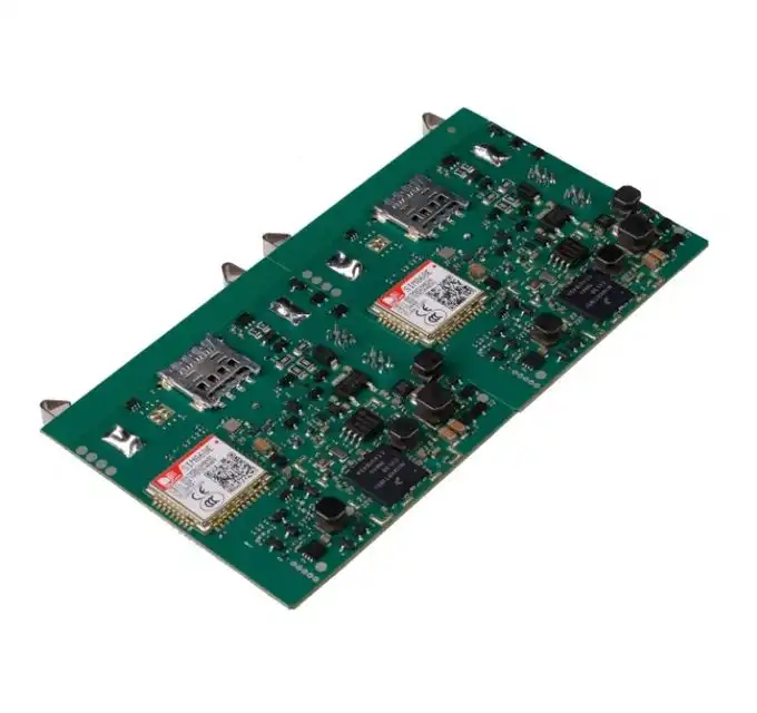
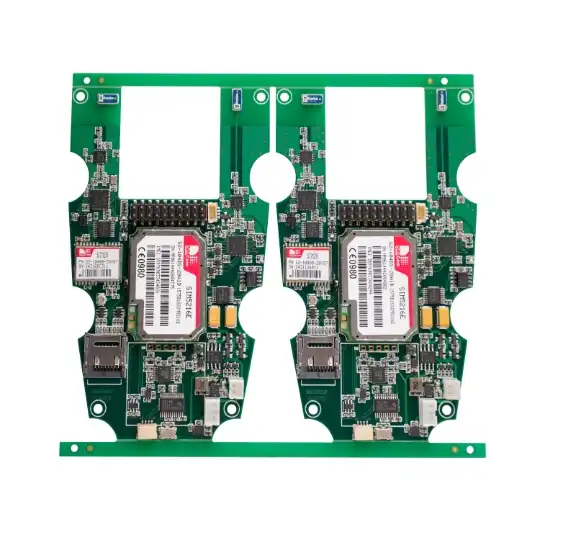
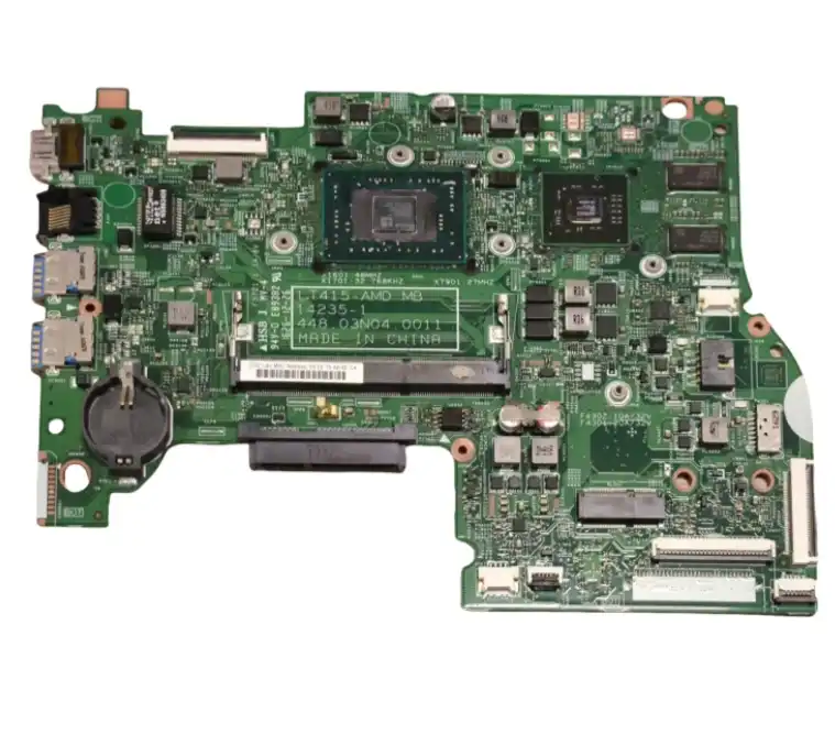
PCB Assembly Solutions for Complex Multilayer Boards
Circuit solutions for modern electronics are getting more complicated, and multilayer PCB assembly has become the standard for high-performance devices in many fields. This high-tech way of making things involves building complicated board structures with many electric layers. This lets designers make small products that work really well. Understanding these assembly methods is important for getting the best product performance and market success whether you're making medical devices, car systems, or telecommunications equipment.
Understanding Multilayer PCB Assembly
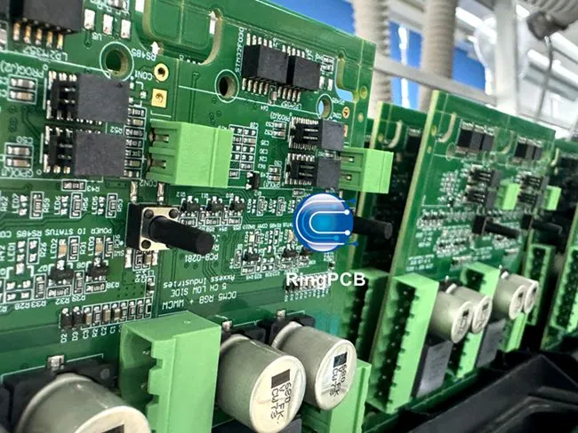
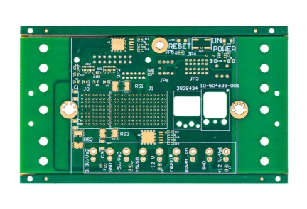
Multilayer PCB assembly is a complex way to make circuit boards with many conductive layers separated by materials that don't carry electricity. Because of this technology, engineers can make small, dense circuits that they couldn't make with regular single- or double-layer boards.
Core Principles of Multi-Layer Construction
Basically, multilayer boards work by stacking layers of electrical copper and insulating base materials on top of each other. Each layer has a specific job to do, such as protecting against radio radiation and distributing power. Through carefully designed vias, which form electrical paths that keep data integrity throughout the board structure, layers are connected to each other.
These days, Multilayer PCB Assembly systems can have anywhere from four to forty-eight layers, based on the needs of the application. The number of layers directly affects how well the board can handle complicated wiring, lower electromagnetic interference, and keep its small size, which is important for today's tiny electronics.
Manufacturing Precision and Performance Benefits
During the assembly process, lamination, cutting, and finishing must be done with great accuracy. Laser drilling is used in advanced manufacturing facilities to make microvias with diameters as small as 0.1mm. This allows for high-density links that support the move toward smaller components.
A good layered system has better electrical performance because it has better control over impedance, less signal crosstalk, and better heat management. Multilayer boards are essential for 5G communication systems and new medical monitoring tools that need to send high-speed signals reliably because of these benefits.
Multilayer PCB Assembly Process and Design Guidelines
There are many important steps in the manufacturing process for multilayer parts that need to be done with great care and strict respect to quality standards throughout the whole cycle.
Step-by-Step Manufacturing Workflow
The first step is to prepare and check the materials. Then, each substrate layer is put through a series of intensive tests to make sure its electrical properties and stability in terms of size meet the requirements. Before moving on to the layup step, the width of the copper foil, the dielectric constant, and the surface roughness are all checked.
When layer stacking, exact technical models are used to show how much copper to use, how thick the prepreg should be, and how many holes need to be drilled. Automated sewing systems are used in more advanced facilities to get rid of human mistake and make sure that registration between layers is always the same. The stacked assembly is then put through controlled processes of high and low temperatures that bond all the layers together permanently.
Computer-controlled tools are used in drilling to make holes that are usually within ±0.05mm of the true size. When drilling, differences in the stack-up must be taken into account, and the hole walls must be kept clean so that metal can stick well in later steps of the process.
Design Optimization Strategies
For layered design to work well, signal integrity, thermal control, and manufacturing limitations need to be carefully thought through. Trace routing rules say how far apart wires must be, and via placement methods make sure that different types of signals are properly separated.
The design of the power and ground planes is very important to how well the board works overall. Putting the planes in the right place lowers electromagnetic interference and makes sure that power is evenly distributed across all circuit parts. To keep electrical performance standards, design engineers have to make sure that the spread of copper is balanced so that it doesn't bend during assembly.
As the number of layers goes up, thermal control issues become more important. By placing thermal vias strategically and paying close attention to copper pour patterns, you can help high-power components get rid of the heat they produce, which stops thermal stress that could damage the reliability over time.
Comparing Multilayer PCB Assembly with Other PCB Types
Knowing the differences between PCB technologies helps buying teams make smart choices based on the needs of the project, the expected performance, and the available budget.
Structural and Performance Differences
Single- and double-layer boards are cheaper for simple circuits, but they can't handle as many routes or as well as multilayer systems can. Because simple boards don't have a lot of space for components, it's often necessary to make the boards bigger to fit complicated circuits.
Multilayer PCB Assembly and rigid-flex assemblies use flexible links between layers of technology to make three-dimensional packaging options possible. This method gives you more design options, but it usually costs more than regular layered structures because it's harder to make and needs special materials.
High-frequency boards use special low-loss materials and impedance-controlled designs that work best for microwave and millimeter-wave uses. Multilayer stack-ups are common on these boards, but they take more design work and higher material costs than normal multilayer assemblies.
Cost-Performance Analysis
Most of the time, layered manufacturing costs more up front than simpler PCB types, but the long-term benefits often make up for the extra cost. Multilayer boards allow for smaller product shapes, higher electricity performance, and better stability, all of which can give companies an edge in tough markets.
Cost patterns are greatly affected by factors like volume. While there may be big price differences between PCB types for prototypes, these differences are usually smaller when a lot of boards are made. This is because industrial savings cancel out the extra costs of materials and processing that come with multilayer construction.
Procuring Multilayer PCB Assembly Services: A B2B Buyer's Guide
To get the best results from your project and a long-lasting relationship, you need to carefully look at the skills, quality systems, and services that each provider offers when you're looking for multilayer assembly services.
Essential Supplier Evaluation Criteria
Quality certificates are one of the most important ways to tell if a provider is capable and reliable. Industry-specific certifications, such as IATF16949 for automotive uses or ISO13485 for medical devices, show that a company knows how to work in regulated markets. ISO9001 certification shows that a company follows quality management principles.
As part of evaluating a company's manufacturing skills, you should look at its equipment specs, layer count limits, and dimensional tolerances. Advanced suppliers keep up-to-date laser cutting systems, automatic optical inspection systems, and flying probe tests that make sure quality is the same no matter how much is made.
When working with complicated multilayer systems, being able to provide technical help becomes very important. Design for manufacturing (DFM) analysis, impedance modeling, and temperature simulation services from suppliers can help improve designs while lowering development risks and accelerating time to market.
Lead Time and Pricing Considerations
Depending on the number of layers and the difficulty of the specifications, prototype lead times for multilayer structures are usually between five and ten days. Schedules for mass production depend on how much is needed and how much ability the provider has. For standard constructions, lead times usually range from two to four weeks.
The way prices are set reflects how complicated layered assembly methods are. The end price is affected by the cost of materials, the number of layers, the type of vias used, and the surface finish standards. Transparent sellers give buyers thorough quotes that break down costs by process step. This helps buyers understand value propositions and find ways to improve things.
Overcoming Challenges in Multilayer PCB Assembly
Complex layered structures are hard to make because they need specialized knowledge, high-tech tools, and thorough quality control systems to make sure the results are reliable.
Common Failure Modes and Prevention Strategies
Delamination is one of the worst ways for layered systems to fail. It usually happens because the layers don't stick together well enough or because of thermal stress during assembly. Some ways to stop this from happening are to choose the right materials, control the lamination parameters, and do thermal cycle tests during the approval stages.
As the number of layers rises and feature sizes fall, accurate registration between levels becomes more and more important. Multilayer PCB Assembly requires optical alignment systems in advanced manufacturing facilities to keep tight registration tolerances throughout the assembly. These systems account for material movement that happens during processing.
To make sure that solder joints in multiple systems work well, you need to pay close attention to how you handle heat and choose the right materials. Because multilayer boards have more thermal mass, they can change how joints are formed and how well soldering profiles work. This means that the process needs to be optimized and full thermal profiling needs to be done during setup.
Advanced Testing and Quality Assurance
Flying probe testing lets you check the electrical integrity of complicated multilayer structures in a thorough way without having to buy expensive test tools. This method covers all electrical tests completely while still being adaptable to prototype and low-volume production needs.
X-ray inspection tools show problems inside a part and the quality of a solder joint that can't be seen with the naked eye. Modern X-ray machines can find holes, inclusions, and alignment problems that could hurt the long-term dependability of something if they are not found.
Functional verification and in-circuit testing make sure that boards that have been put together meet all electrical and performance requirements before they are shipped. Multiple checking methods are used in comprehensive test plans to get defect rates well below industry standards while keeping production moving quickly.
Conclusion
Multilayer PCB assembly is the latest and greatest in circuit board technology. It makes it possible to make small, high-performance solutions for tough electronic tasks. Because multilayer assemblies have complicated manufacturing processes, design issues, and quality standards, it's important to be careful when choosing a supplier and work with experienced manufacturers who have the technical know-how and advanced skills to consistently deliver results.
When buying professionals understand how complicated multilayer assembly is, they can make choices that balance performance needs, cost concerns, and time limits. Investing in good layered assembly services pays off in the long run by making products work better, being more reliable, and giving you an edge in markets that are becoming more complex.
FAQ
What factors determine multilayer PCB assembly lead times?
Lead times depend on a number of important factors, such as the number of layers, the complexity of the board, and the amount of production. It usually takes 5–10 days to make a prototype assembly, but it could take 2–4 weeks for production quantities. Specific needs, like closed vias, rare materials, or tight standards, can make lead times longer. Suppliers who have modern tools and well-organized work processes can often get things done faster without lowering the quality standards.
How do costs compare between different layer counts?
Costs go up in a way that is not straight with the number of layers added. When you go from 4 to 6 layers, prices tend to go up a little, but when you go from 12 layers or more, prices go up a lot. Cost per unit is affected by volume in a big way, with high-volume orders lowering the extra cost increase of extra layers. The end price structures are also affected by the choice of material and the type of via.
What certifications should I look for in a multilayer PCB assembly supplier?
Some important certificates are ISO9001 for managing quality, UL approval for following safety rules, and RoHS certification for meeting environmental standards. Certifications that are specific to an industry, like IATF16949 for automotive, ISO13485 for medical, or AS9100 for aerospace, show that the person has specialized knowledge. IPC qualification shows that you follow the rules for good work and are technically skilled.
What design considerations are most important for multilayer assemblies?
To plan for signal integrity, you need to be very careful with impedance control and layer stack-up design. Problems with reliability can be avoided by placing vias correctly and distributing copper evenly. Electromagnetic efficiency is affected by the design of the power and ground planes. When placing components, assembly limitations and temperature issues must be taken into account. Reviewing the design for manufacturing (DFM) helps find possible output problems early in the development process.
How can I ensure quality in multilayer PCB assembly production?
Quality control starts with making sure that suppliers are qualified and that key performance indicators are constantly being watched. Electrical proof, dimensional checking, and reliability testing should all be part of thorough testing plans. Performance standards are kept up by regularly auditing and reviewing suppliers' work. Specifications and acceptance standards that are clear help avoid confusion and make sure that all production runs produce the same results.
Partner with Ring PCB for Superior Multilayer PCB Assembly Solutions
Ring PCB Technology offers complete multilayer PCB manufacturing services that are designed to meet the specific needs of modern electronics makers. Our cutting edge building can handle complicated layered structures with up to 48 layers and more accuracy and dependability than the norm in the industry. With ISO9001, IATF16949, and ISO13485 certifications, we offer stable quality and low prices to a wide range of businesses, such as automotive, medical, and telecommunications. Get in touch with our engineering team at [email protected] to talk about your multilayer PCB assembly needs and find out why top makers trust Ring PCB as their multilayer PCB assembly supplier.
References
1. Smith, J.R., "Advanced Multilayer PCB Design Techniques for High-Speed Applications," Electronic Manufacturing Review, 2023, Vol. 45, pp. 112-128.
2. Chen, L., Wang, M., "Quality Control Methods in Multilayer PCB Assembly Manufacturing," International Journal of PCB Technology, 2023, Vol. 18, No. 3, pp. 45-62.
3. Thompson, K.A., "Cost Analysis and Optimization Strategies for Multilayer PCB Production," Manufacturing Technology Quarterly, 2022, Vol. 31, pp. 78-94.
4. Rodriguez, S., "Thermal Management in Complex Multilayer PCB Assemblies," IEEE Transactions on Electronics Manufacturing, 2023, Vol. 46, No. 2, pp. 156-171.
5. Anderson, P.J., "Procurement Best Practices for Multilayer PCB Assembly Services," Supply Chain Management in Electronics, 2023, pp. 234-251.
6. Liu, X., "Reliability Testing Methods for Multilayer PCB Assembly Validation," Quality Assurance in Electronic Manufacturing, 2022, Vol. 29, No. 4, pp. 89-105.

Welcome to Ring PCB! Share your inquiry, and receive a tailored quotation!

Ring PCB, your trusted partner for PCB & PCBA Full Turnkey Solutions
