Custom Communication PCBA Solutions for Your Business
In today's rapidly evolving technological landscape, custom Communication PCBA (Printed Circuit Board Assembly) solutions are essential for businesses seeking to stay ahead of the curve. These tailored circuit boards form the backbone of modern communication devices, enabling seamless connectivity and data transfer across various platforms. By opting for custom Communication PCBA solutions, companies can enhance their product performance, reduce costs, and accelerate time-to-market. Whether you're developing cutting-edge mobile devices, sophisticated networking equipment, or innovative IoT solutions, partnering with a reliable PCBA manufacturer can provide the competitive edge your business needs in the dynamic world of communications technology.
The Importance of Custom Communication PCBA
The Role of Communication PCBA in Modern Devices
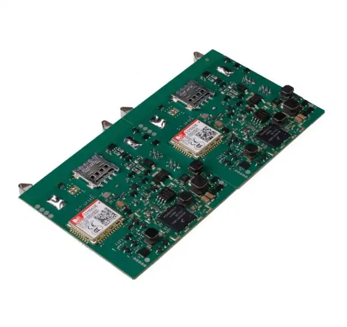
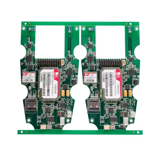
Communication PCBA serves as the nervous system of modern communication devices, facilitating the transmission and reception of data across various platforms. These specialized circuit boards are crucial components in a wide array of devices, including smartphones, routers, satellite systems, and IoT devices. The intricate design and layout of Communication PCBA enable efficient signal processing, ensuring that information flows seamlessly between different parts of a device or across networks.
One of the key advantages of Communication PCBA is its ability to integrate multiple functions into a single, compact board. This integration not only reduces the overall size of devices but also enhances their performance and reliability. For instance, a single Communication PCBA can handle tasks such as signal amplification, modulation, and data encryption, all while maintaining high-speed connectivity.

Benefits of Customization in Communication PCBA
Opting for custom Communication PCBA solutions offers numerous benefits for businesses in the telecommunications sector. Customization allows companies to tailor the circuit board design to their specific requirements, optimizing performance for particular applications. This level of flexibility is particularly valuable in an industry where innovation and differentiation are key drivers of success.
Custom Communication PCBA can also lead to significant cost savings in the long run. By designing boards that are optimized for specific products, companies can reduce material waste, improve energy efficiency, and minimize the need for additional components. Moreover, customization allows for better space utilization within devices, potentially reducing the overall size and weight of the final product.
Key Considerations in Designing Custom Communication PCBA
Selecting the Right Materials and Components
The choice of materials and components plays a crucial role in the performance and reliability of Communication PCBA. High-frequency applications, common in modern communication devices, require materials with low dielectric loss and controlled impedance. FR-4, a glass-reinforced epoxy laminate material, is widely used for its excellent electrical and mechanical properties. However, for more demanding applications, advanced materials like Rogers or PTFE-based laminates may be necessary.
Component selection is equally critical. Factors such as operating frequency, power consumption, and environmental conditions must be carefully considered. For instance, high-speed communication devices may require specialized ICs (Integrated Circuits) and passive components designed for GHz frequencies. Additionally, the increasing demand for miniaturization has led to the adoption of advanced packaging technologies like BGA (Ball Grid Array) and QFN (Quad Flat No-leads), which offer higher component density and improved electrical performance.
Optimizing Layout and Signal Integrity
The layout of a Communication PCBA is crucial for ensuring optimal signal integrity and minimizing electromagnetic interference (EMI). Proper trace routing, controlled impedance design, and effective ground plane implementation are essential techniques for maintaining signal quality. Designers must carefully consider factors such as trace width, spacing, and layer stack-up to achieve the desired impedance and reduce signal reflections.
Advanced design techniques like differential signaling and microstrip or stripline transmission lines are often employed in high-speed Communication PCBA. These methods help maintain signal integrity over longer distances and at higher frequencies. Additionally, the strategic placement of components and the use of proper shielding techniques can significantly reduce EMI, ensuring that the PCBA meets regulatory standards and performs reliably in real-world conditions.
Manufacturing and Quality Assurance for Communication PCBA
Advanced Manufacturing Techniques
The production of high-quality Communication PCBA requires advanced manufacturing techniques and state-of-the-art equipment. Precision pick-and-place machines are used to accurately position components on the board, while reflow soldering ensures reliable connections. For more complex designs, techniques like wave soldering or selective soldering may be employed for through-hole components.
Surface finish is another critical aspect of Communication PCBA manufacturing. Finishes like ENIG (Electroless Nickel Immersion Gold) or HASL (Hot Air Solder Leveling) are commonly used to protect exposed copper surfaces and ensure good solderability. The choice of surface finish can impact the board's performance, especially in high-frequency applications where skin effect and surface roughness play significant roles.
Rigorous Testing and Quality Control
Quality assurance is paramount in Communication PCBA manufacturing. Rigorous testing procedures are implemented to ensure that each board meets the required specifications and performs reliably under various conditions. Automated Optical Inspection (AOI) systems are used to detect visual defects, while In-Circuit Testing (ICT) verifies the electrical integrity of the assembled board.
For high-frequency Communication PCBA, additional tests like Vector Network Analysis (VNA) may be performed to characterize the board's RF performance. Environmental stress screening, including thermal cycling and vibration testing, helps identify potential reliability issues before the boards are integrated into final products. These comprehensive quality control measures are essential for ensuring that Communication PCBA meets the stringent requirements of modern communication devices.
Conclusion
Custom Communication PCBA solutions offer businesses the flexibility and performance needed to excel in the competitive telecommunications market. By carefully considering material selection, design optimization, and manufacturing processes, companies can create Communication PCBA that meets their specific requirements while ensuring reliability and cost-effectiveness. As technology continues to evolve, partnering with experienced PCBA manufacturers becomes increasingly crucial for staying at the forefront of communication innovation.
Lead-Free Communication PCBA Compliant with Global Standards
Ring PCB Technology Co., Limited, your trusted PCB Manufacturing Partner since 2008, offers comprehensive one-stop services for Communication PCBA. With our self-owned factory and full supply chain control, we ensure vertical integration from raw material procurement to production and testing. Our triple quality assurance process, including AOI, impedance testing, and thermal cycling, results in a defect rate of <0.2%, surpassing the industry average. We proudly hold global certifications such as ISO9001, IATF16949, and RoHS compliance.
For businesses looking to leverage the power of custom Communication PCBA, reaching out to specialized manufacturers can be the first step towards achieving technological excellence. For more information on custom Communication PCBA solutions tailored to your business needs, contact us at [email protected].
References
1. Smith, J. (2022). Advanced Printed Circuit Board Design and Manufacturing Techniques for Communication Devices. IEEE Communications Magazine, 60(4), 78-85.
2. Johnson, R. A., & Cheng, L. (2021). Custom PCBA Solutions in the Era of 5G: Challenges and Opportunities. Journal of Telecommunications and Information Technology, 3, 45-52.
3. Williams, E. M., & Brown, K. L. (2023). Optimizing Communication PCBA for IoT Applications: A Comprehensive Guide. International Journal of Electronics and Communications, 142, 154083.
4. Chen, Y., & Liu, X. (2020). High-Frequency PCB Design Techniques for Next-Generation Communication Systems. IEEE Transactions on Components, Packaging and Manufacturing Technology, 10(7), 1162-1173.
5. Thompson, S. D., & Garcia, M. A. (2022). Quality Assurance Methodologies in Custom PCBA Manufacturing for Telecommunication Industries. Quality Engineering, 34(2), 200-212.

Welcome to Ring PCB! Share your inquiry, and receive a tailored quotation!

Ring PCB, your trusted partner for PCB & PCBA Full Turnkey Solutions


