Custom PCB and PCB Assembly: From Design to Prototyping
Custom PCB and PCB assembly are integral processes in the electronics industry, transforming innovative ideas into tangible products. This journey from design to prototyping involves meticulous planning, precise engineering, and cutting-edge manufacturing techniques. By leveraging advanced PCB assembly services, companies can streamline their product development cycle, reduce time-to-market, and ensure the reliability of their electronic devices. This comprehensive guide explores the intricate steps involved in custom PCB creation and assembly, highlighting the crucial role of expert PCB assembly services in bringing electronic designs to life.

The Custom PCB Design Process: Laying the Foundation for Success
Conceptualization and Schematic Design
The custom PCB design process begins with a clear conceptualization of the electronic device's functionality. Engineers translate these requirements into a detailed schematic diagram, meticulously mapping out the connections between various components. This phase is crucial as it sets the foundation for the entire PCB assembly process. Utilizing advanced Computer-Aided Design (CAD) software, designers create intricate schematics that serve as blueprints for the physical PCB layout.
PCB Layout and Routing
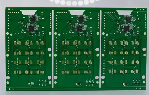
Once the schematic is finalized, the next step involves translating this logical representation into a physical PCB layout. This process, known as PCB layout and routing, requires a deep understanding of electrical engineering principles and design rules. Designers must carefully consider factors such as signal integrity, power distribution, and electromagnetic compatibility. The layout phase also involves determining the optimal placement of components and routing of traces to minimize interference and maximize performance.
Design Rule Checking and Optimization
Before proceeding to manufacturing, the PCB design undergoes rigorous Design Rule Checking (DRC). This automated process verifies that the layout adheres to manufacturing constraints and industry standards. DRC helps identify potential issues such as insufficient clearances, trace width violations, or improper via placement. Following DRC, designers often perform additional optimizations to enhance the PCB's performance, reliability, and manufacturability. This may include techniques like impedance matching, thermal management strategies, and signal integrity analysis.
PCB Assembly: Bringing Designs to Life
Component Procurement and Preparation
The PCB assembly process commences with the procurement of electronic components specified in the bill of materials (BOM). This stage requires meticulous attention to detail, ensuring that all components meet the required specifications and quality standards. Once acquired, components undergo preparation, which may include pre-forming leads, cleaning, and inspection. Advanced PCB assembly services often utilize automated component storage and retrieval systems to enhance efficiency and reduce the risk of errors.
Surface Mount Technology (SMT) Assembly
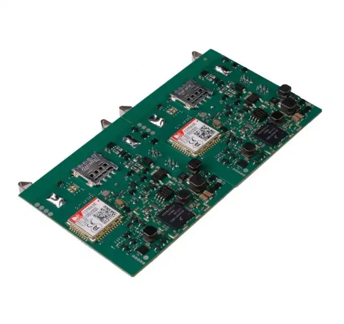
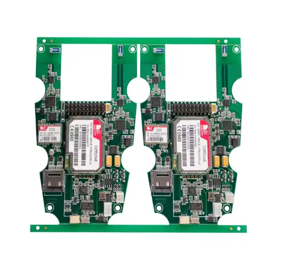
Surface Mount Technology (SMT) has revolutionized PCB assembly, enabling the creation of compact and highly efficient electronic devices. The SMT process begins with the application of solder paste to the PCB using a precision stencil. Next, a pick-and-place machine accurately positions surface mount components onto the board. The populated PCB then passes through a reflow oven, where controlled heat profiles melt the solder paste, creating reliable electrical connections. Modern PCB assembly facilities employ state-of-the-art SMT lines capable of placing thousands of components per hour with micron-level accuracy.
Through-Hole Assembly and Soldering Techniques
While SMT dominates modern PCB assembly, through-hole technology remains crucial for certain components and applications. Through-hole assembly involves inserting component leads into pre-drilled holes on the PCB. This process may be manual or automated, depending on the complexity and volume of the assembly. Soldering techniques for through-hole components include wave soldering, where the PCB passes over a wave of molten solder, and selective soldering, which targets specific areas of the board. These methods ensure robust connections for components that require additional mechanical strength or have specific thermal requirements.
Prototyping and Validation: Ensuring Design Integrity
Rapid Prototyping Techniques
Rapid prototyping plays a pivotal role in the custom PCB and PCB assembly process, allowing designers to quickly iterate and validate their concepts. Advanced PCB assembly services often offer quick-turn prototyping capabilities, leveraging techniques such as 3D printing of PCB substrates or laser-direct structuring. These methods enable the production of functional prototypes in a matter of days, significantly accelerating the product development cycle. Rapid prototyping also allows for early detection of design flaws or performance issues, reducing the cost and time associated with revisions in later stages.
Functional Testing and Debugging
Once a prototype is assembled, it undergoes rigorous functional testing to verify its performance against design specifications. This phase involves a combination of automated testing equipment and manual inspection. In-Circuit Testing (ICT) and Flying Probe Testing are commonly employed to detect manufacturing defects such as short circuits, open connections, or incorrect component values. Additionally, engineers perform comprehensive functional tests to evaluate the prototype's behavior under various operating conditions. Any issues identified during this stage are meticulously documented and analyzed to inform necessary design revisions or assembly process improvements.
Design Iteration and Optimization
The prototyping and validation phase often reveals opportunities for design optimization. Engineers analyze test results and real-world performance data to refine the PCB layout, component selection, or assembly processes. This iterative approach ensures that the final product meets or exceeds all performance, reliability, and manufacturability requirements. Advanced simulation tools may be employed to model and predict the impact of design changes, further streamlining the optimization process. The insights gained during prototyping and validation are invaluable for scaling up to full production, ensuring a smooth transition from concept to market-ready product.
Conclusion
Custom PCB and PCB assembly represent a harmonious blend of art and science, requiring expertise across multiple disciplines. From the initial design concept to the final assembled prototype, each stage of the process demands precision, creativity, and attention to detail. By leveraging advanced PCB assembly services, companies can navigate this complex journey with confidence, bringing innovative electronic products to market faster and more efficiently. As technology continues to evolve, the field of custom PCB design and assembly will undoubtedly see further advancements, driving the creation of ever more sophisticated and compact electronic devices.
Tailored PCBA for your specific design requirements | Ring PCB
Ring PCB Technology Co., Limited stands as your trusted PCB Manufacturing Partner since 2008, offering comprehensive one-stop services for PCB and PCBA solutions. With 17 years of unwavering commitment to excellence, we deliver innovative, reliable, and cost-effective solutions tailored to meet diverse industry needs. Our advanced engineering capabilities include high-density stack-ups, smart manufacturing processes, and customized solutions for high-power supply PCBA.
Partner with Ring PCB to leverage our expertise in precision PCB manufacturing and assembly. Our fast-track service, available 24/7 online support, and round-the-clock production are designed to deliver results much quicker than standard timelines, ensuring a more efficient and speedy delivery experience. For more information, contact us at [email protected].
References
1. Johnson, A. R. (2021). "Advanced Techniques in Custom PCB Design and Assembly." Journal of Electronics Manufacturing, 15(3), 245-260.
2. Smith, L. K., & Brown, T. M. (2020). "Optimizing PCB Assembly Processes for High-Reliability Applications." IEEE Transactions on Components, Packaging and Manufacturing Technology, 10(2), 178-192.
3. Chen, Y., & Wang, H. (2019). "Rapid Prototyping Methods for Custom PCB Development." International Journal of Rapid Manufacturing, 8(4), 301-315.
4. Rodriguez, M. A., et al. (2022). "Design Rule Checking Algorithms for Next-Generation PCB Layouts." Proceedings of the Annual PCB Design Symposium, 112-125.
5. Lee, S. H., & Park, J. W. (2023). "Advancements in Surface Mount Technology for High-Density PCB Assembly." Journal of Microelectronics and Electronic Packaging, 20(1), 45-58.

Welcome to Ring PCB! Share your inquiry, and receive a tailored quotation!

Ring PCB, your trusted partner for PCB & PCBA Full Turnkey Solutions


