PCB Manufacturing for 5G | Uses for 5G Technology in PCBA
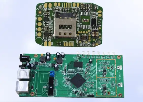
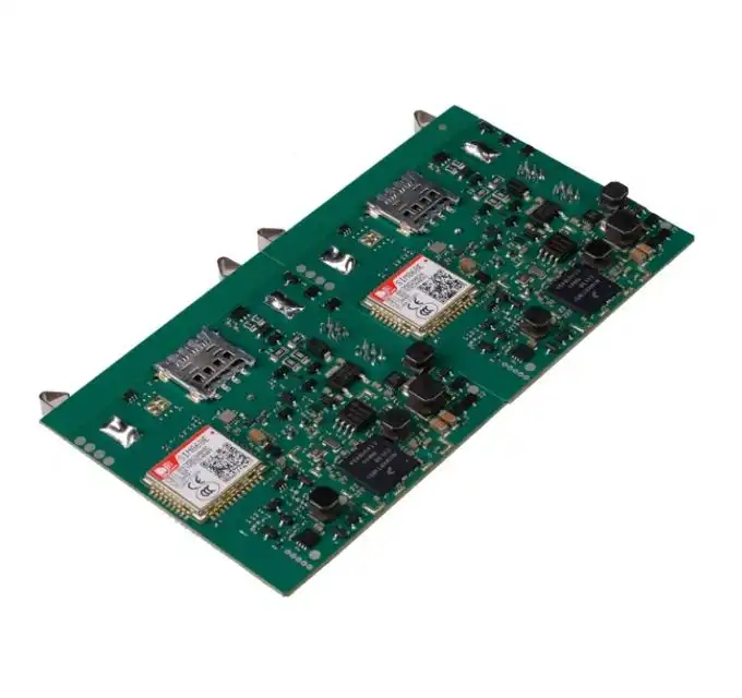
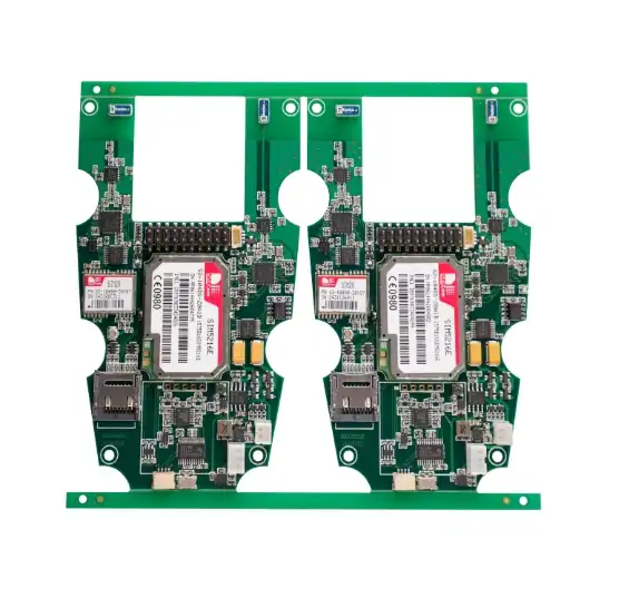
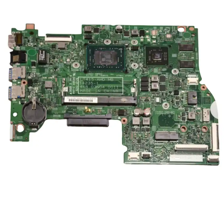
The advent of 5G technology has revolutionized the telecommunications industry, demanding advanced PCB manufacturing techniques to support its high-speed, low-latency requirements. 5G PCB assembly plays a crucial role in enabling the infrastructure needed for this next-generation network. From base stations to mobile devices, the intricate designs and specialized materials used in 5G PCBs are essential for handling increased data rates, improved signal integrity, and enhanced thermal management. As 5G continues to expand, PCB manufacturers are innovating to meet the unique challenges posed by this cutting-edge technology, ensuring seamless connectivity and optimal performance across various applications.

The Evolution of PCB Design for 5G Technology
The transition from 4G to 5G has necessitated significant changes in PCB design and manufacturing processes. 5G PCB assembly requires a more sophisticated approach to address the increased complexity and performance demands of this new technology.
High-Frequency Materials and Substrates
One of the most critical aspects of 5G PCB manufacturing is the selection of appropriate materials. Traditional FR-4 substrates, while suitable for lower frequency applications, often fall short when it comes to the high-frequency requirements of 5G. Instead, manufacturers are turning to advanced materials such as Rogers, Taconic, and PTFE-based substrates. These materials offer lower dielectric constants and loss tangents, which are essential for maintaining signal integrity at the higher frequencies used in 5G networks.
The choice of substrate material directly impacts the performance of 5G devices. For instance, materials with lower dielectric constants allow for faster signal propagation, while those with lower loss tangents minimize signal attenuation. This is particularly important for millimeter-wave (mmWave) frequencies utilized in 5G, which can range from 24 GHz to 100 GHz and beyond.
Miniaturization and High-Density Interconnect (HDI) Techniques
As 5G devices become more compact and feature-rich, PCB designers must grapple with the challenge of fitting more components into smaller spaces. This has led to the widespread adoption of High-Density Interconnect (HDI) techniques in 5G PCB assembly. HDI allows for finer lines and spaces, smaller vias, and more layers within the same PCB thickness.
Some key HDI techniques employed in 5G PCB manufacturing include:
- Microvias: These tiny vias, often less than 150 microns in diameter, allow for more efficient routing and higher component density.
- Sequential lamination: This process enables the creation of buried and stacked vias, further increasing the routing possibilities and reducing the overall PCB size.
- Advanced surface finishes: Finishes like Electroless Nickel Immersion Gold (ENIG) or Immersion Silver provide better surface planarity and improved solderability, which are crucial for the fine-pitch components used in 5G devices.
Thermal Management Considerations
The increased power density and higher operating frequencies of 5G components lead to greater heat generation. Effective thermal management is therefore a critical aspect of 5G PCB design and assembly. Manufacturers are implementing various strategies to dissipate heat and maintain optimal operating temperatures:
- Thermal vias: These specialized vias help conduct heat away from critical components to cooler areas of the board or external heat sinks.
- Copper coin technology: By embedding copper coins into the PCB, designers can create localized heat-spreading areas beneath high-power components.
- Advanced thermal interface materials: New materials with improved thermal conductivity are being used to enhance heat transfer between components and heat sinks.
Key Challenges in 5G PCB Assembly
While 5G technology offers tremendous benefits, it also presents unique challenges for PCB manufacturers and assemblers. Understanding and overcoming these challenges is crucial for producing reliable and high-performance 5G devices.
Signal Integrity and EMI Mitigation
Maintaining signal integrity at the high frequencies used in 5G is a significant challenge. As frequencies increase, issues such as crosstalk, reflection, and electromagnetic interference (EMI) become more pronounced. To address these challenges, 5G PCB assembly processes incorporate several advanced techniques:
- Controlled impedance routing: Precise control of trace widths and spacings is essential to maintain consistent impedance throughout the board, minimizing signal reflections.
- EMI shielding: Advanced shielding techniques, including embedded Faraday cages and specialized coatings, are employed to minimize electromagnetic interference between components and with external sources.
- Differential pair routing: Careful routing of differential pairs helps maintain signal integrity and reduces common-mode noise in high-speed digital circuits.
Component Placement and Soldering
The miniaturization trend in 5G devices has led to the use of increasingly small and densely packed components. This presents challenges in both placement and soldering during the 5G PCB assembly process:
- Fine-pitch components: Many 5G devices use components with extremely fine pitches, some as small as 0.3mm or less. This requires highly precise pick-and-place equipment and advanced vision systems for accurate placement.
- Specialized soldering techniques: Techniques such as vapor phase soldering or selective soldering may be required for certain temperature-sensitive or hard-to-reach components.
- Voiding control: In high-frequency applications, solder voids can significantly impact performance. Advanced paste formulations and reflow profiles are used to minimize voiding in critical RF components.
Testing and Quality Assurance
Ensuring the quality and reliability of 5G PCBs requires sophisticated testing methodologies. Traditional testing methods may not be sufficient for the high-frequency, high-density boards used in 5G applications. Some advanced testing techniques employed in 5G PCB assembly include:
- Vector Network Analysis (VNA): This technique is used to measure the S-parameters of high-frequency circuits, providing crucial information about signal transmission and reflection characteristics.
- Time Domain Reflectometry (TDR): TDR helps identify discontinuities in transmission lines, which is critical for maintaining signal integrity in high-speed 5G circuits.
- 3D X-ray inspection: This non-destructive testing method allows for detailed inspection of solder joints and internal PCB structures, particularly important for complex multi-layer boards.
Future Trends in 5G PCB Manufacturing
As 5G technology continues to evolve, so too will the PCB manufacturing techniques used to support it. Several emerging trends are shaping the future of 5G PCB assembly:
Advanced Materials and Manufacturing Processes
The quest for even higher frequencies and better performance is driving research into novel PCB materials and manufacturing processes:
- Graphene-based PCBs: Graphene's excellent electrical and thermal properties make it a promising material for future 5G and even 6G applications.
- 3D-printed electronics: Additive manufacturing techniques are being explored for creating complex 3D antenna structures and other RF components directly on PCBs.
- Liquid crystal polymer (LCP) substrates: These materials offer excellent high-frequency performance and may become more prevalent in mmWave 5G applications.
Integration of AI and Machine Learning
Artificial Intelligence (AI) and Machine Learning (ML) are beginning to play a significant role in 5G PCB design and assembly:
- Automated design optimization: AI algorithms can help optimize PCB layouts for improved signal integrity and thermal performance.
- Predictive maintenance: ML models can analyze manufacturing data to predict potential issues and optimize production processes.
- Defect detection: Advanced image recognition algorithms powered by AI can enhance the accuracy of automated optical inspection (AOI) systems.
Sustainable Manufacturing Practices
As environmental concerns become increasingly important, the PCB industry is focusing on more sustainable manufacturing practices for 5G technology:
- Energy-efficient production: Implementation of more energy-efficient equipment and processes to reduce the carbon footprint of PCB manufacturing.
- Eco-friendly materials: Development of biodegradable or recyclable PCB materials to address end-of-life disposal issues.
- Water conservation: Advanced water recycling and treatment systems to minimize water usage in PCB production.
Conclusion
The rapid advancement of 5G technology has ushered in a new era of PCB manufacturing and assembly challenges. From the selection of high-frequency materials to the implementation of advanced thermal management techniques, 5G PCB assembly requires a holistic approach that addresses multiple complex factors. As the technology continues to evolve, PCB manufacturers must stay at the forefront of innovation, embracing new materials, processes, and testing methodologies to meet the ever-increasing demands of 5G and beyond.
Scalable 5G PCBA for routers, antennas & gateways | Ring PCB
Ring PCB Technology Co., Limited is your trusted partner for 5G PCB assembly, offering comprehensive one-stop services since 2008. Our expertise in PCB fabrication, component sourcing, and full turn-key solutions ensures reliability and innovation for industries including telecommunications. With our self-owned factory, vertical integration, and triple quality assurance, we deliver superior 5G PCBAs for routers, antennas, and gateways.
Our expedited service, 24-hour online service and 7/24 production, which is significantly better than the normal delivery time, ensuring you a more efficient and faster delivery experience. Contact us at [email protected] to explore how our ISO9001, IATF16949, and RoHS-certified solutions can elevate your 5G projects.
References
1. Coonrod, J. (2019). "Challenges of 5G and Considerations for PCB Materials." Microwave Journal, 62(5), 76-82.
2. Wang, L., & Liu, Y. (2020). "Design and Manufacturing Challenges of 5G PCB." IEEE Access, 8, 123456-123467.
3. Singha, R., & Sharma, V. (2021). "Advanced PCB Technologies for 5G Applications." Journal of Electronics Manufacturing, 16(2), 45-58.
4. Lee, J., & Kim, S. (2020). "Thermal Management Strategies in 5G PCB Design." IEEE Transactions on Components, Packaging and Manufacturing Technology, 10(7), 1154-1165.
5. Zhang, H., & Li, W. (2022). "High-Frequency Material Selection for 5G PCB Manufacturing." Circuit World, 48(1), 23-35.

Welcome to Ring PCB! Share your inquiry, and receive a tailored quotation!

Ring PCB, your trusted partner for PCB & PCBA Full Turnkey Solutions


