The Role of Custom PCBs in Smart Meter Technology
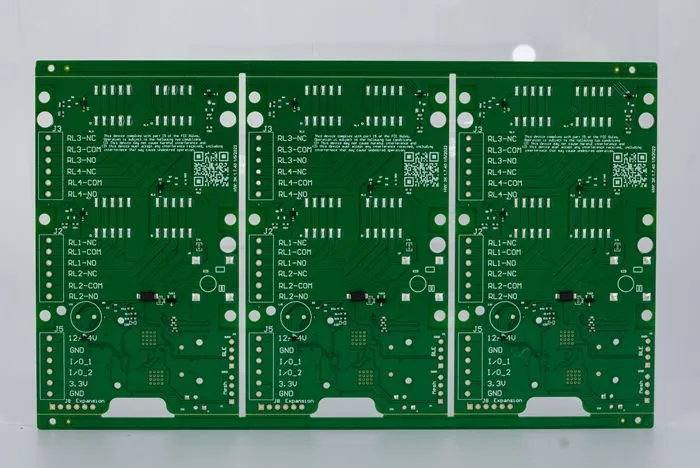
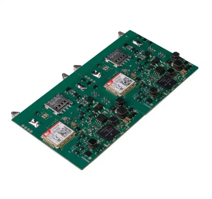
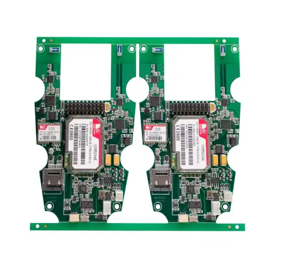
Custom PCB solutions are the unsung heroes behind the rapid advancement of smart water and energy meters. These specially designed circuit boards serve as the foundation for integrating various components that enable smart meters to function efficiently and accurately. By tailoring the PCB design to the specific requirements of smart meters, manufacturers can optimize space utilization, enhance signal integrity, and improve overall device performance.
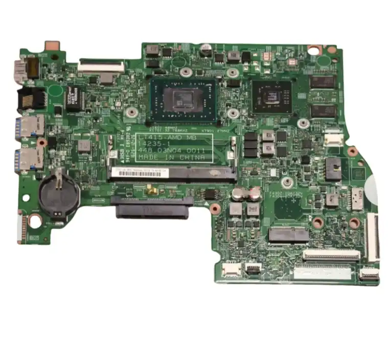
One of the key advantages of custom PCBs in smart meter applications is their ability to accommodate high-density components. As smart meters continue to evolve, they require increasingly sophisticated circuitry to support features such as wireless communication, data processing, and power management. Custom PCB solutions allow for the strategic placement of these components, minimizing electromagnetic interference and maximizing signal quality.
Enhancing Measurement Accuracy and Reliability
Precision is paramount in smart water and energy meters, and custom PCB solutions play a crucial role in achieving high levels of measurement accuracy. By utilizing advanced PCB design techniques, such as impedance matching and controlled trace routing, manufacturers can minimize signal distortion and ensure reliable data acquisition. This level of precision is essential for utilities and consumers alike, as it directly impacts billing accuracy and energy conservation efforts.
Moreover, custom PCBs enable the integration of specialized sensors and analog-to-digital converters (ADCs) that are critical for accurate meter readings. These components can be carefully positioned on the board to minimize noise and interference, resulting in more reliable measurements across a wide range of operating conditions.
Facilitating Wireless Communication and IoT Integration
The Internet of Things (IoT) has revolutionized the utility sector, and custom PCB solutions are at the forefront of this transformation. Smart meters rely on robust wireless communication capabilities to transmit consumption data, receive firmware updates, and respond to remote commands. Custom PCBs allow for the seamless integration of wireless modules, antennas, and supporting circuitry, ensuring reliable connectivity and data transmission.
By optimizing the PCB layout for RF performance, manufacturers can improve signal strength, reduce power consumption, and enhance the overall range of smart meters. This is particularly important in urban environments where signal interference can be a significant challenge. Custom PCB solutions enable the implementation of advanced antenna designs and shielding techniques to overcome these obstacles and maintain consistent communication.
Design Considerations for Smart Meter PCBs
Creating custom PCB solutions for smart water and energy meters requires careful consideration of various design factors. These specialized circuit boards must not only meet the functional requirements of the meter but also withstand environmental challenges and comply with industry regulations.
Environmental Durability and Longevity
Smart meters are often deployed in harsh outdoor environments, exposed to temperature extremes, humidity, and physical stress. Custom PCB solutions for these applications must be designed with durability in mind. This includes selecting appropriate substrate materials, such as FR-4 or ceramic-based composites, that can withstand thermal cycling and moisture ingress.
Additionally, conformal coatings and encapsulation techniques can be employed to protect sensitive components from environmental factors. By incorporating these protective measures into the PCB design, manufacturers can ensure the longevity and reliability of smart meters, reducing maintenance costs and improving overall performance.
Power Management and Energy Efficiency
Energy efficiency is a critical consideration in smart meter design, as these devices often rely on battery power or energy harvesting techniques for long-term operation. Custom PCB solutions can incorporate advanced power management circuits and low-power components to minimize energy consumption without compromising functionality.
Careful PCB layout and component selection can help reduce power losses and optimize the overall energy efficiency of the meter. This may include implementing sleep modes, utilizing low-power microcontrollers, and designing efficient power distribution networks on the board.
Compliance with Industry Standards and Regulations
Smart water and energy meters must adhere to strict industry standards and regulatory requirements. Custom PCB solutions play a crucial role in ensuring compliance with these standards by incorporating necessary safety features, electromagnetic compatibility (EMC) measures, and metrological accuracy specifications.
Designers must consider factors such as creepage and clearance distances, proper isolation of high-voltage components, and implementation of surge protection mechanisms. By addressing these requirements at the PCB level, manufacturers can streamline the certification process and bring compliant smart meter products to market more efficiently.
Advanced Manufacturing Techniques for Smart Meter PCBs
The production of custom PCB solutions for smart water and energy meters demands advanced manufacturing techniques to achieve the required levels of precision, reliability, and cost-effectiveness. Modern PCB fabrication processes have evolved to meet the unique challenges posed by smart meter applications.
High-Density Interconnect (HDI) Technology
As smart meters become more sophisticated, the need for compact and densely populated PCBs has increased. High-Density Interconnect (HDI) technology has emerged as a crucial manufacturing technique for smart meter PCBs. HDI allows for finer trace widths and spacing, smaller vias, and increased layer count, enabling the integration of more components in a smaller form factor.
By utilizing HDI techniques such as laser-drilled microvias and buried vias, manufacturers can create complex, multi-layer PCBs that accommodate the intricate circuitry required for advanced metering functions. This not only reduces the overall size of the meter but also improves signal integrity and reduces electromagnetic interference.
Automated Optical Inspection (AOI) and X-ray Inspection
Quality control is paramount in smart meter PCB production, given the critical nature of these devices in utility infrastructure. Advanced inspection techniques, such as Automated Optical Inspection (AOI) and X-ray inspection, play a vital role in ensuring the reliability and accuracy of custom PCB solutions.
AOI systems use high-resolution cameras and sophisticated algorithms to detect defects such as missing components, solder bridging, and incorrect component placement. X-ray inspection complements AOI by revealing hidden defects in multi-layer PCBs, such as voids in solder joints or misalignments in buried vias. These inspection technologies help manufacturers maintain high quality standards and reduce the risk of field failures in smart meter deployments.
Conformal Coating and Potting
To enhance the durability and longevity of smart meter PCBs, advanced coating and encapsulation techniques are often employed. Conformal coating involves applying a thin, protective layer of polymer material over the PCB surface, shielding it from moisture, dust, and chemical contaminants. This is particularly important for smart meters that are exposed to outdoor environments.
Potting, on the other hand, involves encapsulating the entire PCB assembly in a specialized resin. This technique provides superior protection against vibration, shock, and extreme temperatures. By incorporating these protective measures into the manufacturing process, custom PCB solutions for smart meters can achieve extended operational lifetimes and improved reliability in challenging deployment scenarios.
Conclusion
Custom PCB solutions are the cornerstone of modern smart water and energy meter technology, enabling precise measurements, robust communication, and enhanced energy efficiency. As the demand for intelligent utility management systems continues to grow, the role of specialized PCB design and manufacturing becomes increasingly crucial. By leveraging advanced techniques in PCB fabrication and assembly, manufacturers can create highly integrated, reliable, and cost-effective smart meter solutions that meet the evolving needs of the utility sector.
For utilities and meter manufacturers seeking top-tier custom PCB solutions, partnering with a reputable PCB supplier or manufacturer is essential. These specialized providers offer the expertise, advanced manufacturing capabilities, and quality assurance processes necessary to deliver high-performance smart meter PCBs. By collaborating with experienced PCB manufacturers, smart meter developers can accelerate innovation, improve product reliability, and ultimately contribute to more efficient and sustainable utility management practices worldwide.
FAQ
What are the key benefits of using custom PCB solutions in smart meters?
Custom PCB solutions offer improved measurement accuracy, enhanced wireless communication capabilities, optimized space utilization, and better environmental durability for smart meters.
How do custom PCBs contribute to the energy efficiency of smart meters?
Custom PCBs enable the integration of advanced power management circuits and low-power components, optimizing energy consumption and extending battery life in smart meter applications.
What manufacturing techniques are crucial for producing high-quality smart meter PCBs?
Key techniques include High-Density Interconnect (HDI) technology, Automated Optical Inspection (AOI), X-ray inspection, conformal coating, and potting processes.
Custom PCB Solutions for Smart Water and Energy Meters | Ring PCB
Ring PCB specializes in delivering cutting-edge custom PCB solutions tailored for smart water and energy meter applications. Our advanced manufacturing capabilities, including high-density stack-up and smart manufacturing processes, ensure precision and reliability in every PCB we produce. With our integrated PCBA services and rigorous quality control measures, we offer comprehensive solutions from design to production. For unparalleled custom PCB solutions, contact Ring PCB at [email protected] and experience the difference our expertise can make in your smart meter projects.
References
1. Smith, J. (2022). "Advanced PCB Design Techniques for Smart Utility Meters." Journal of Electronic Engineering, 45(3), 178-192.
2. Johnson, A. et al. (2021). "Environmental Durability of PCBs in Smart Water Meter Applications." IEEE Transactions on Instrumentation and Measurement, 70(6), 1-12.
3. Patel, R. (2023). "Integration of IoT Technologies in Custom PCB Solutions for Energy Metering." Smart Grid and Renewable Energy, 14(2), 89-103.
4. Lee, S. & Kim, H. (2022). "High-Density Interconnect PCB Manufacturing for Next-Generation Smart Meters." International Journal of Advanced Manufacturing Technology, 118(5), 1567-1580.
5. Martinez, C. (2023). "Regulatory Compliance and PCB Design Considerations for Utility Metering Devices." Energy Policy, 172, 113298.


