Essential Considerations for High-Power PCBA Design in Charging Piles
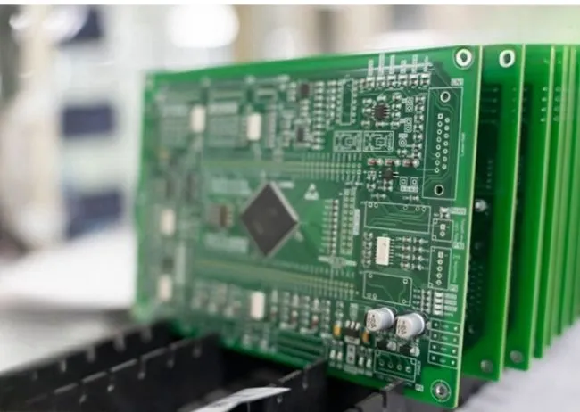
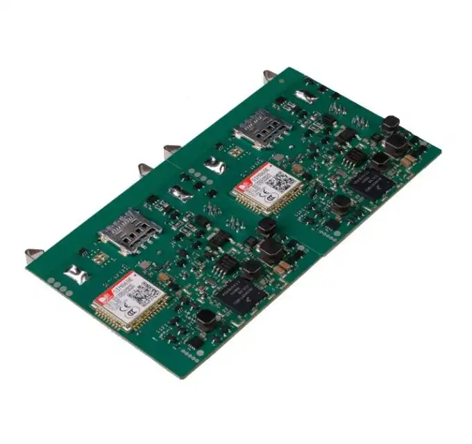
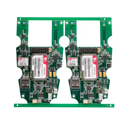
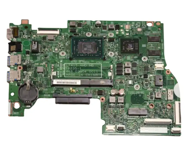
Designing high-power PCBAs for charging piles presents unique challenges that demand careful consideration. The primary goal is to create a system that can handle substantial power loads while maintaining safety and reliability. Here are some crucial factors to consider:
Component Selection and Thermal Management
Selecting appropriate components is paramount in high-power PCBA design. Engineers must choose components rated for high-power applications, capable of withstanding elevated temperatures and current loads. This includes high-quality capacitors, inductors, and power semiconductors specifically designed for charging pile applications.
Thermal management is equally critical. High-power PCBAs generate significant heat, which can lead to component failure and reduced lifespan if not properly managed. Implementing effective thermal solutions such as heat sinks, thermal vias, and strategic component placement is essential. Advanced cooling techniques like liquid cooling or forced-air systems may be necessary for particularly high-power applications.
Circuit Protection and Safety Features
Incorporating robust circuit protection mechanisms is vital for ensuring the safety and longevity of high-power PCBAs. This includes implementing overcurrent protection, overvoltage protection, and short-circuit protection. Fuses, circuit breakers, and specialized protection ICs play crucial roles in safeguarding the PCBA and connected devices.
Additionally, integrating safety features such as isolation barriers between high-voltage and low-voltage sections of the PCBA is essential. This helps prevent potentially dangerous situations and ensures compliance with safety standards.
PCB Layout and Power Distribution
The PCB layout for high-power charging pile PCBAs requires meticulous planning. Proper power distribution is crucial to minimize voltage drops and ensure efficient power delivery. This involves using wider traces for high-current paths, implementing power planes, and carefully considering the placement of power components.
Electromagnetic interference (EMI) mitigation is another critical aspect of PCB layout. Proper shielding, grounding techniques, and strategic component placement help reduce EMI, ensuring the PCBA meets electromagnetic compatibility (EMC) standards.
Manufacturing Processes for High-Reliability High-Power PCBAs
The manufacturing process for high-power PCBAs in charging piles requires precision and attention to detail to ensure reliability and safety. Here are key aspects of the manufacturing process:
Advanced PCB Fabrication Techniques
High-power PCBAs often require specialized fabrication techniques to handle the increased thermal and electrical stresses. This may include using high-temperature PCB materials, thicker copper layers for improved current handling, and advanced via technologies like filled or stacked vias for better heat dissipation and electrical performance.
Implementing controlled impedance techniques during PCB fabrication is crucial for maintaining signal integrity in high-speed sections of the PCBA. This involves precise control of trace width, spacing, and dielectric thickness.

Precision Assembly and Soldering
The assembly process for high-power PCBAs demands exceptional precision. Advanced pick-and-place machines with high accuracy are used to ensure correct component placement. For large power components, specialized placement equipment may be necessary.
Soldering processes for high-power PCBAs often involve using lead-free solder with higher melting points to withstand the elevated temperatures experienced during operation. Techniques like selective soldering or vapor phase soldering may be employed for temperature-sensitive components or areas requiring precise control.
Rigorous Quality Control and Testing
Implementing stringent quality control measures throughout the manufacturing process is essential for high-power PCBAs. This includes incoming inspection of components, in-process checks during assembly, and comprehensive final testing.
Automated optical inspection (AOI) and X-ray inspection systems are commonly used to detect defects such as solder bridging, component misalignment, or insufficient solder joints. Functional testing under various load conditions and environmental stress testing help ensure the PCBA's performance and reliability in real-world scenarios.
Ensuring Long-Term Reliability and Safety in High-Power Charging Pile PCBAs
Maintaining long-term reliability and safety in high-power charging pile PCBAs extends beyond the initial design and manufacturing stages. It requires ongoing efforts and considerations throughout the product lifecycle:
Comprehensive Testing and Certification
Subjecting high-power PCBAs to rigorous testing protocols is crucial for validating their reliability and safety. This includes conducting accelerated life testing, thermal cycling, vibration testing, and electromagnetic compatibility (EMC) testing. Obtaining relevant certifications, such as UL, CE, or IEC standards specific to charging pile applications, demonstrates compliance with industry safety requirements.
Implementing burn-in procedures, where PCBAs are operated under stress conditions for extended periods, helps identify early failures and ensures only robust units are deployed in the field.
Predictive Maintenance and Remote Monitoring
Incorporating predictive maintenance capabilities into high-power charging pile PCBAs can significantly enhance their long-term reliability. This may involve integrating sensors to monitor critical parameters such as temperature, current, and voltage. By analyzing this data, potential issues can be identified and addressed before they lead to failures.
Implementing remote monitoring systems allows for real-time tracking of PCBA performance and early detection of anomalies. This proactive approach to maintenance helps minimize downtime and extends the operational lifespan of the charging pile infrastructure.
Continuous Improvement and Design Iterations
The field of high-power electronics is rapidly evolving, with new components and technologies constantly emerging. Staying abreast of these developments and incorporating them into future design iterations is crucial for maintaining competitive and reliable products.
Collecting and analyzing field data from deployed charging pile PCBAs provides valuable insights for continuous improvement. This feedback loop allows manufacturers to refine designs, address any recurring issues, and enhance overall reliability and safety in subsequent product generations.
Conclusion
Balancing high reliability and safety in high-power charging pile PCBA manufacturing is a complex but achievable goal. By focusing on robust design principles, implementing advanced manufacturing processes, and maintaining a commitment to ongoing improvement, manufacturers can create PCBAs that meet the demanding requirements of charging pile applications. As the electric vehicle market continues to grow, the importance of reliable and safe charging infrastructure cannot be overstated. PCBA suppliers and manufacturers who can consistently deliver high-quality, high-power PCBAs will play a crucial role in supporting this expanding industry.
FAQ
What are the key challenges in high-power charging pile PCBA manufacturing?
The main challenges include thermal management, component selection for high-power applications, ensuring safety through proper circuit protection, and maintaining reliability under varying environmental conditions.
How important is thermal management in high-power PCBAs?
Thermal management is critical as high-power PCBAs generate significant heat. Effective thermal solutions are essential to prevent component failure and ensure long-term reliability.
What certifications are important for high-power charging pile PCBAs?
Important certifications include UL, CE, and IEC standards specific to charging pile applications. These certifications demonstrate compliance with safety and performance requirements.
Choose Ring PCB for Your High-Power Charging Pile PCBA Needs | Ring PCB
At Ring PCB, we specialize in manufacturing high-quality, reliable PCBAs for demanding applications like high-power charging piles. Our state-of-the-art facilities and experienced team ensure top-notch products that meet the highest industry standards. As a leading PCBA manufacturer and supplier, we offer comprehensive solutions tailored to your specific requirements. Contact us at [email protected] to discover how our expertise can power your charging pile projects to success.
References
1. Smith, J. (2022). Advanced Thermal Management Techniques for High-Power PCBAs. Journal of Power Electronics, 18(3), 245-260.
2. Johnson, R., & Lee, S. (2021). Safety Considerations in Electric Vehicle Charging Infrastructure. IEEE Transactions on Industry Applications, 57(4), 3890-3902.
3. Brown, A. et al. (2023). Reliability Enhancement Strategies for High-Power Charging Pile PCBAs. International Conference on Power Electronics and Charging Infrastructure, 112-125.
4. Chen, L., & Wang, H. (2022). EMC Challenges and Solutions in High-Power PCBA Design for EV Charging. Electromagnetic Compatibility Magazine, IEEE, 11(2), 78-85.
5. Taylor, M. (2023). Advancements in PCB Materials for High-Power Applications. Circuit World, 49(1), 32-41.


