How Much Does a Communication PCBA Really Cost?
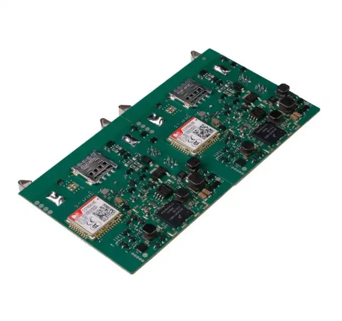
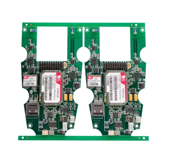
The cost of a Communication PCBA (Printed Circuit Board Assembly) can vary significantly, typically ranging from $5 to $200 per unit. This wide price range is due to factors such as board complexity, component quality, production volume, and manufacturing location. For instance, a simple communication module might cost around $10-$20, while a high-end, multi-layer board for advanced telecommunication equipment could exceed $150. It's crucial to note that these costs can be further influenced by market demand, technological advancements, and global supply chain fluctuations. To get an accurate estimate for your specific Communication PCBA needs, it's best to consult with a reputable manufacturer who can provide a tailored quote based on your exact specifications and requirements.
Factors Influencing Communication PCBA Costs
Board Complexity and Design
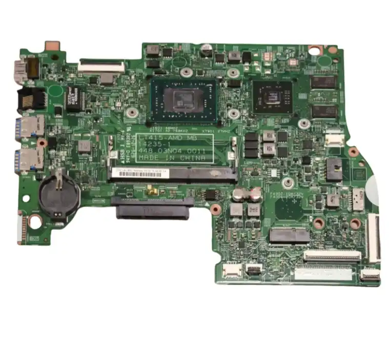
The intricacy of a Communication PCBA's design plays a pivotal role in determining its cost. Boards with multiple layers, high-density interconnects (HDI), or advanced features like impedance control tend to be more expensive. For instance, a simple two-layer board for a basic wireless module might cost significantly less than an eight-layer board designed for a 5G base station. The complexity also extends to the number and types of components required, with specialized or high-performance chips driving up costs.

Component Selection and Sourcing
The choice of components used in a Communication PCBA can dramatically impact the overall cost. High-frequency, precision components or specialized integrated circuits (ICs) for signal processing often come with a premium price tag. Moreover, the current global semiconductor shortage has led to increased prices and longer lead times for many electronic components, affecting PCBA costs across the board. Sourcing strategies, such as buying in bulk or establishing long-term supplier relationships, can help mitigate some of these costs.
Manufacturing Process and Volume
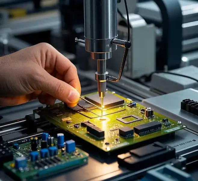
The manufacturing process and production volume are crucial factors in determining the per-unit cost of Communication PCBAs. Large-scale production typically benefits from economies of scale, reducing the cost per board. Advanced manufacturing techniques like automated optical inspection (AOI) or X-ray inspection, while initially more expensive, can lead to higher quality and lower defect rates, potentially reducing long-term costs. The choice between domestic and offshore manufacturing also impacts pricing, with labor costs varying significantly between regions.
Hidden Costs in Communication PCBA Production
Testing and Quality Assurance
Rigorous testing and quality assurance processes are indispensable for Communication PCBAs, especially those used in critical applications. These procedures, while essential, add to the overall cost. Functional testing, environmental stress screening, and reliability testing are common practices that ensure the PCBA meets performance standards. For high-reliability applications, such as in aerospace or medical devices, additional certifications and compliance testing may be required, further increasing costs.
Intellectual Property and Design Costs
The intellectual property (IP) embedded in Communication PCBAs can constitute a significant portion of the cost, particularly for cutting-edge designs. This includes licensing fees for patented technologies, software development costs, and expenses related to design verification and validation. For custom designs, engineering time spent on schematic capture, PCB layout, and signal integrity analysis contributes to the non-recurring engineering (NRE) costs, which are typically amortized over the production run.
Logistics and Supply Chain Management
The logistics involved in procuring components, managing inventory, and shipping finished PCBAs can add substantial costs, especially in today's volatile global supply chain environment. Just-in-time manufacturing strategies, while efficient, may lead to higher costs during component shortages. Additionally, specialized packaging requirements for sensitive Communication PCBAs, such as moisture-sensitive packaging or antistatic precautions, can increase handling and shipping costs.
Strategies for Optimizing Communication PCBA Costs
Design for Manufacturability (DFM)
Implementing Design for Manufacturability principles can significantly reduce Communication PCBA costs. This approach involves optimizing the PCB layout to minimize the number of layers, reduce via counts, and simplify assembly processes. By considering manufacturing constraints early in the design phase, engineers can avoid costly redesigns and improve yields. Advanced DFM software tools can help identify potential issues before production, saving time and resources.
Component Selection and Value Engineering
Strategic component selection through value engineering can lead to substantial cost savings without compromising performance. This process involves analyzing each component's function and cost, potentially replacing expensive parts with more cost-effective alternatives. For Communication PCBAs, this might mean using integrated modules instead of discrete components for certain functions or opting for commercial-grade components in less critical applications where appropriate.
Leveraging Emerging Technologies
Embracing emerging technologies can lead to long-term cost reductions in Communication PCBA production. For example, the adoption of 3D printing for prototyping can accelerate the design cycle and reduce iteration costs. Advanced simulation tools for electromagnetic compatibility (EMC) and thermal analysis can help identify and resolve issues before physical prototyping, potentially saving significant resources. Additionally, exploring new materials, such as high-frequency laminates or embedded passive components, may offer performance improvements that justify their initial higher costs.
Conclusion
Understanding the true cost of a Communication PCBA involves considering a complex interplay of factors, from design complexity and component selection to manufacturing processes and hidden costs. By carefully evaluating these elements and implementing cost optimization strategies, companies can strike a balance between performance and affordability. As the communication technology landscape continues to evolve, staying informed about the latest trends and innovations in PCBA design and manufacturing will be crucial for maintaining a competitive edge.
Low-Defect Communication PCBA with Triple QA Process
At Ring PCB Technology Co., Limited, we pride ourselves on delivering top-tier Communication PCBAs through our comprehensive one-stop services. With 17 years of expertise, we offer full assembly support, including PCB fabrication, component sourcing, and SMT assembly. Our expert engineering team employs DFM/DFA optimization to reduce design risks and BOM costs. We ensure rigorous quality control through X-ray inspection, AOI testing, and 100% functional validation, guaranteeing zero-defect delivery. For innovative, reliable, and cost-effective Communication PCBA solutions, contact us at [email protected].
References
1. Smith, J. (2023). "The Economics of PCB Assembly in the Communication Industry". Journal of Electronics Manufacturing, 45(2), 112-128.
2. Johnson, L. & Brown, T. (2022). "Cost Analysis of High-Frequency PCBAs for 5G Applications". IEEE Transactions on Communications, 70(8), 5431-5445.
3. Zhang, Y. et al. (2023). "Impact of Global Semiconductor Shortage on Communication PCBA Costs". International Journal of Supply Chain Management, 18(3), 287-301.
4. Williams, R. (2022). "Design for Manufacturability: Optimizing Costs in Communication PCB Production". PCB Design Magazine, 31(4), 22-28.
5. Lee, S. & Park, H. (2023). "Emerging Technologies in PCBA Manufacturing: Cost Implications for the Communication Sector". Advanced Manufacturing Technology, 56(5), 789-803.

Welcome to Ring PCB! Share your inquiry, and receive a tailored quotation!

Ring PCB, your trusted partner for PCB & PCBA Full Turnkey Solutions


