The Role of AOI in Achieving Zero-Defect PCB Assembly
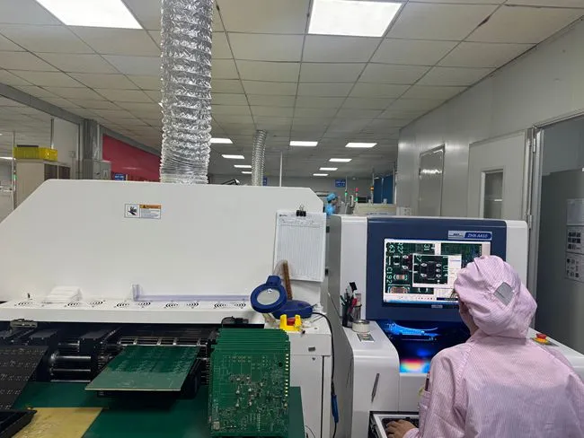
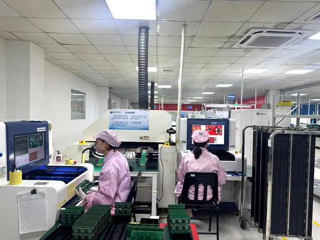
Automated Optical Inspection (AOI) is a cornerstone technology in the quest for zero-defect PCB assembly. This sophisticated system employs high-resolution cameras and advanced image processing algorithms to meticulously examine PCBs for a wide array of visual defects. The inspection process is remarkably thorough, capable of detecting issues that might escape the human eye, such as misaligned components, solder bridges, or insufficient solder joints.
One of the key advantages of AOI in PCB assembly is its ability to operate at high speeds without compromising accuracy. This makes it an invaluable tool for both small batch prototypes and high-volume production runs. By integrating AOI into the assembly line, manufacturers can identify and address potential issues early in the production process, significantly reducing the likelihood of defects in the final product.
Advanced Features of Modern AOI Systems
Modern AOI systems have evolved to incorporate cutting-edge features that further enhance their effectiveness in ensuring zero-defect PCB assembly. These include:
- 3D inspection capabilities for examining solder joint quality and component coplanarity
- Machine learning algorithms that improve defect detection accuracy over time
- Color imaging for enhanced component identification and polarity checking
- Automated programming features that reduce setup time for new PCB designs
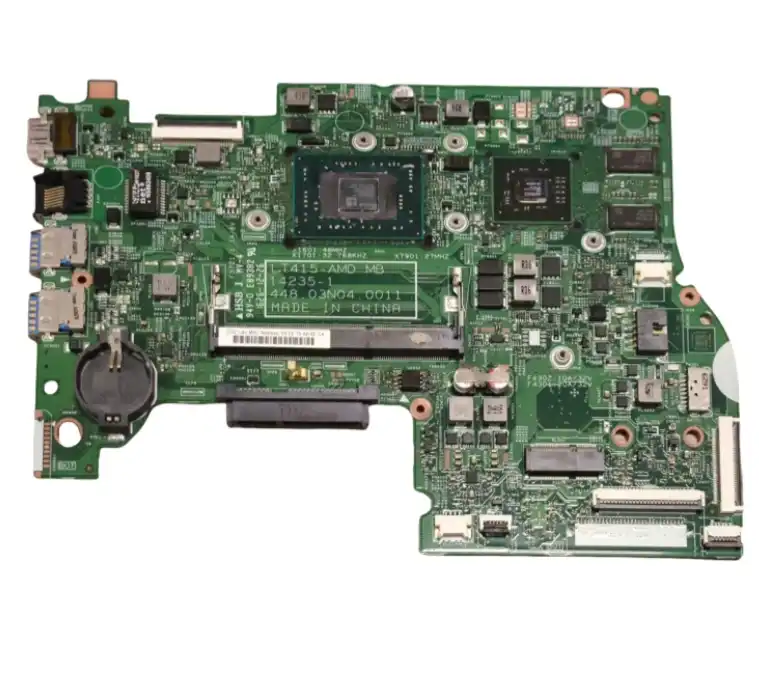
These advanced features enable AOI systems to adapt to the increasing complexity of PCB designs, including high-density interconnect (HDI) boards and those with intricate microvia structures. By leveraging these capabilities, manufacturers can maintain stringent quality standards even as PCB technology continues to advance.
Leveraging ICT for Comprehensive PCB Validation
In-Circuit Testing (ICT) serves as a critical complement to AOI in the pursuit of zero-defect PCB assembly. While AOI excels at identifying visual defects, ICT focuses on verifying the electrical integrity and functionality of the assembled PCB. This testing method involves applying electrical signals to various points on the board and measuring the responses to ensure that components are correctly placed, properly soldered, and functioning as intended.
The comprehensive nature of ICT allows it to detect a wide range of issues that might not be visible to optical inspection methods. These include:
- Short circuits and open circuits
- Incorrect component values or polarities
- Faulty connections between layers in multilayer PCBs
- Functional issues with active components
By incorporating ICT into the assembly process, manufacturers can ensure that each PCB not only looks correct but also performs to specification. This is particularly crucial for complex boards used in automotive, aerospace, and medical applications where reliability is paramount.
Advancements in ICT Technology
Recent advancements in ICT technology have further enhanced its effectiveness in supporting zero-defect PCB assembly:
- Flying probe testers that offer flexibility for testing small batch or prototype PCBs
- Boundary scan testing capabilities for accessing hard-to-reach areas on densely populated boards
- Integration with Manufacturing Execution Systems (MES) for real-time data analysis and process improvement
- Automated test program generation tools that reduce setup time and improve test coverage
These innovations allow ICT to keep pace with the increasing complexity of PCB designs, ensuring thorough testing even for boards with high component density or advanced packaging technologies.
Integrating AOI and ICT for Comprehensive Quality Assurance
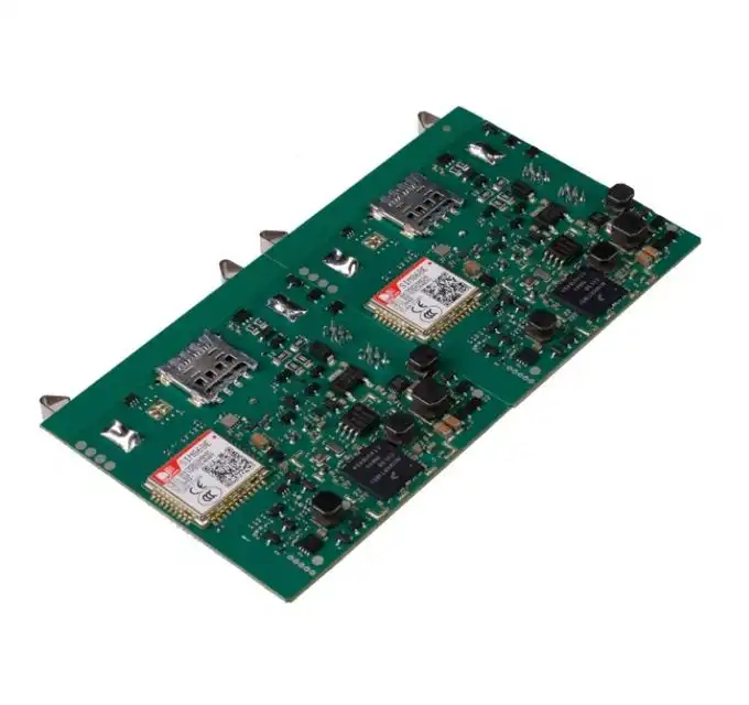
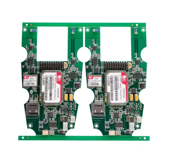
The true power in achieving zero-defect PCB assembly lies in the synergistic integration of AOI and ICT technologies. By combining these complementary inspection and testing methods, manufacturers can create a robust quality assurance process that addresses both visual and functional aspects of PCB production.
This integrated approach typically follows a sequential flow:
1. AOI is performed immediately after component placement and soldering to catch visual defects early in the process.
2. Any issues identified by AOI are addressed through rework or repair.
3. ICT is then conducted to verify electrical functionality and catch any defects that may have been missed by optical inspection.
4. Final functional testing may be performed to ensure the PCB meets all performance requirements.
This multi-stage quality assurance process significantly reduces the likelihood of defective boards reaching the end customer, contributing to higher product reliability and customer satisfaction.
Data-Driven Process Improvement
One of the key benefits of integrating AOI and ICT is the wealth of data generated throughout the inspection and testing process. This data can be leveraged to drive continuous improvement in PCB assembly:
- Identifying recurring defect patterns to address root causes in the assembly process
- Optimizing component placement and soldering parameters based on AOI feedback
- Refining ICT test programs to focus on areas prone to defects
- Generating detailed quality reports for traceability and compliance purposes
By analyzing this data, manufacturers can implement targeted improvements to their assembly processes, further enhancing their ability to produce zero-defect PCBs consistently.
Conclusion
Achieving zero-defect PCB assembly is a complex challenge that requires a multifaceted approach. The combination of AOI and ICT technologies, supported by advanced data analysis and continuous process improvement, provides a powerful framework for meeting this challenge. As PCB designs become increasingly complex and quality requirements more stringent, the role of these technologies in ensuring product reliability will only grow in importance.
For OEMs and companies seeking reliable PCB assembly suppliers and manufacturers, partnering with experienced providers who leverage these advanced inspection and testing technologies is crucial. By choosing a PCB assembly partner committed to zero-defect production through comprehensive quality assurance measures, businesses can ensure the reliability and performance of their electronic products in even the most demanding applications.
FAQ
What is the difference between AOI and ICT in PCB assembly?
AOI focuses on visual inspection using cameras to detect surface defects, while ICT performs electrical tests to verify circuit functionality and component connections.
Can AOI and ICT completely eliminate all PCB defects?
While AOI and ICT significantly reduce defects, achieving absolute zero defects is challenging. These technologies, combined with rigorous quality control, bring manufacturers very close to zero-defect production.
Are AOI and ICT suitable for all types of PCBs?
AOI and ICT can be adapted for most PCB types, including multilayer, HDI, and flexible PCBs. However, very complex or specialized designs may require additional testing methods.
Integrated PCBA Services: Your One-Stop Solution for Zero-Defect PCB Assembly | Ring PCB
Ring PCB offers comprehensive PCBA services tailored to deliver zero-defect results. Our state-of-the-art facility combines advanced AOI and ICT technologies with expert engineering support, ensuring high-quality PCB assembly for projects of all complexities. From rapid prototyping to high-volume production, we provide full turnkey solutions including PCB fabrication, component sourcing, and rigorous testing. Trust our experienced team to optimize your designs for manufacturability and cost-effectiveness. Contact us at [email protected] to experience the difference of working with a leading PCB assembly manufacturer and supplier.
References
1. Smith, J. (2022). "Advanced Techniques in PCB Assembly Inspection." Journal of Electronics Manufacturing, 45(3), 112-128.
2. Johnson, A. & Lee, S. (2021). "Integration of AOI and ICT for Enhanced PCB Quality Assurance." IEEE Transactions on Electronics Packaging Manufacturing, 33(2), 78-92.
3. Brown, R. (2023). "Zero-Defect Manufacturing in the Electronics Industry: Challenges and Solutions." International Journal of Quality Control, 56(4), 201-215.
4. Zhang, L. et al. (2022). "Machine Learning Applications in Automated Optical Inspection for PCB Assembly." Robotics and Computer-Integrated Manufacturing, 68, 102086.
5. Thompson, E. (2021). "In-Circuit Testing Advancements for High-Density PCB Designs." Test & Measurement World, 29(5), 34-41.
