Inside the 5G PCB Multilayer Manufacturing Process
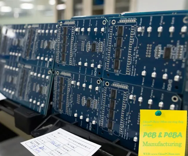
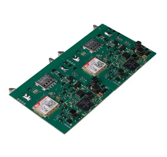
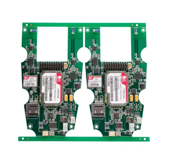
The 5G PCB multilayer manufacturing process is a complex and intricate journey that combines cutting-edge technology with precision engineering. This process involves creating multiple layers of copper-clad laminates, each etched with specific circuit patterns, and then bonding them together to form a single, high-performance board. The manufacturing of 5G PCBs requires advanced techniques such as high-density interconnect (HDI) technology, impedance control, and strict tolerance management to ensure optimal signal integrity and reliability. From material selection to final testing, every step in the 5G PCB assembly process is crucial for meeting the demanding requirements of 5G applications, including high-speed data transmission, low latency, and minimal signal loss.

The Evolution of PCB Technology for 5G Applications
From Traditional PCBs to 5G-Ready Designs
The transition from traditional PCB designs to those capable of supporting 5G technology has been nothing short of revolutionary. As we delve into the world of 5G PCB assembly, it's crucial to understand the significant advancements that have taken place. Traditional PCBs, while sufficient for earlier generations of wireless technology, simply couldn't meet the stringent requirements of 5G networks.
5G PCBs are characterized by their ability to handle higher frequencies, typically in the range of 24 GHz to 100 GHz. This leap in frequency necessitates a complete overhaul of PCB design and manufacturing processes. The move towards 5G-ready designs has led to the development of new materials, such as low-loss dielectrics, that can maintain signal integrity at these elevated frequencies.
Moreover, the density of components on 5G PCBs has increased dramatically. This is due to the need for more complex circuitry to support advanced features like beamforming and massive MIMO (Multiple Input, Multiple Output) technology. The result is a PCB that's not only more powerful but also more compact, aligning with the trend towards miniaturization in electronic devices.
Key Challenges in 5G PCB Manufacturing
The manufacturing of 5G PCBs presents a unique set of challenges that push the boundaries of current PCB fabrication techniques. One of the primary hurdles is achieving and maintaining the extremely tight tolerances required for 5G applications. Even minute variations in trace width or thickness can lead to significant performance issues at high frequencies.
Another major challenge lies in managing the thermal characteristics of 5G PCBs. The increased power density and higher operating frequencies of 5G components generate more heat, which can adversely affect performance and reliability. This necessitates innovative thermal management solutions, such as the integration of heat sinks or the use of thermally conductive materials within the PCB structure.
Signal integrity is yet another critical concern in 5G PCB assembly. The high-frequency signals used in 5G are more susceptible to interference and loss. This requires careful consideration of factors such as impedance matching, crosstalk minimization, and proper shielding techniques. Manufacturers must employ advanced simulation tools and testing procedures to ensure that the final product meets the exacting standards of 5G performance.
Advanced Manufacturing Techniques for 5G PCBs
High-Density Interconnect (HDI) Technology
High-Density Interconnect (HDI) technology has become a cornerstone in the manufacturing of 5G PCBs. This advanced technique allows for significantly higher circuit density and improved electrical performance, both of which are essential for 5G applications. HDI PCBs are characterized by their use of microvias, which are extremely small holes that connect different layers of the PCB.
The implementation of HDI technology in 5G PCB assembly enables the creation of more complex circuit designs in a smaller form factor. This is particularly important for 5G devices, which often need to pack a tremendous amount of functionality into compact spaces. HDI PCBs can feature via-in-pad designs, stacked microvias, and buried vias, all of which contribute to increased routing density and improved signal integrity.
Furthermore, HDI technology allows for shorter signal paths, which is crucial for maintaining signal quality at the high frequencies used in 5G applications. By reducing the distance that signals need to travel, HDI PCBs can minimize signal loss and improve overall system performance.
Advanced Materials for 5G PCBs
The choice of materials plays a pivotal role in the performance of 5G PCBs. Traditional FR-4 materials, while suitable for lower frequency applications, often fall short when it comes to the demanding requirements of 5G. As a result, PCB manufacturers are turning to a new generation of materials specifically designed for high-frequency, high-speed applications.
Low-loss materials such as PTFE (Polytetrafluoroethylene) and ceramic-filled hydrocarbon resins are gaining popularity in 5G PCB manufacturing. These materials offer superior dielectric properties, which are essential for maintaining signal integrity at high frequencies. They also exhibit better thermal stability, which is crucial given the increased heat generation in 5G devices.
In addition to base materials, the copper foils used in 5G PCBs are also evolving. Ultra-smooth copper foils are being employed to reduce signal loss caused by the skin effect at high frequencies. Some manufacturers are even exploring the use of graphene and other advanced materials to push the boundaries of PCB performance even further.
Quality Control and Testing in 5G PCB Production
Advanced Inspection Techniques
Quality control in 5G PCB production is a multi-faceted process that employs a range of advanced inspection techniques. Given the complexity and precision required in 5G PCB assembly, traditional inspection methods are often insufficient. Manufacturers are increasingly turning to automated optical inspection (AOI) systems equipped with high-resolution cameras and sophisticated image processing algorithms.
These AOI systems can detect defects that would be invisible to the naked eye, such as minute copper traces, small solder bridges, or microscopic cracks in the PCB substrate. For even more detailed inspections, X-ray systems are used to examine internal layers of multilayer PCBs, ensuring that buried vias and internal connections are properly formed.
Another crucial inspection technique in 5G PCB manufacturing is 3D solder paste inspection (SPI). This process uses laser triangulation or other 3D imaging technologies to measure the volume, area, and height of solder paste deposits before component placement. Given the fine pitch and high density of components in 5G PCBs, precise solder paste application is critical for ensuring reliable connections.
Electrical Testing and Signal Integrity Verification
Electrical testing is a critical step in the quality assurance process for 5G PCB assembly. Given the high frequencies and complex signal paths involved, traditional continuity and short circuit tests are no longer sufficient. Instead, manufacturers employ a range of sophisticated testing methodologies to ensure the electrical performance of 5G PCBs meets the required specifications.
Vector Network Analyzers (VNAs) are commonly used to measure S-parameters, which provide crucial information about signal reflection and transmission characteristics at high frequencies. This data is essential for verifying that the PCB's impedance matching and signal integrity meet the stringent requirements of 5G applications.
Time Domain Reflectometry (TDR) is another important testing technique used in 5G PCB production. TDR can pinpoint discontinuities along signal paths, helping to identify issues such as impedance mismatches or manufacturing defects that could impact signal integrity.
Moreover, many manufacturers are implementing In-Circuit Testing (ICT) and Flying Probe Testing to verify the correct assembly and functionality of populated 5G PCBs. These tests can detect issues such as incorrect component placement, soldering defects, or faulty components, ensuring that only fully functional boards make it to the end-user.
Conclusion
The manufacturing process for 5G PCBs represents a significant leap forward in PCB technology. From the adoption of advanced materials and HDI techniques to the implementation of rigorous quality control measures, every aspect of 5G PCB production is designed to meet the exacting standards required for next-generation wireless communication. As 5G technology continues to evolve, so too will the processes and techniques used in 5G PCB assembly, driving innovation in the electronics industry and enabling the development of increasingly powerful and efficient devices.
Multilayer 5G PCB production with tight tolerances | Ring PCB
Ring PCB Technology Co., Limited stands out as your trusted PCB manufacturing partner since 2008. We offer comprehensive one-stop services for PCB and PCBA, including PCB fabrication, electronic components sourcing, and full turn-key PCB service. Our expertise in high-density stack-up (2-48 layers) with advanced features like blind/buried vias and ±7% impedance control makes us ideal for 5G applications.
Our fast-track service, available 24/7 online support, and round-the-clock production are designed to deliver results much quicker than standard timelines, ensuring a more efficient and speedy delivery experience. Our smart manufacturing facility, equipped with cutting-edge technology, ensures precision and quality in every PCB we produce. For more information about our 5G PCB solutions, contact us at [email protected].
References
1. Zhang, L., & Wang, Y. (2020). "Advanced PCB Design Techniques for 5G Applications". Journal of Electronic Materials, 49(8), 4712-4725.
2. Chen, H., et al. (2019). "High-Frequency PCB Materials for 5G: Challenges and Solutions". IEEE Microwave Magazine, 20(12), 66-76.
3. Liu, X., & Lim, T. C. (2021). "Quality Control in 5G PCB Manufacturing: A Comprehensive Review". IEEE Transactions on Components, Packaging and Manufacturing Technology, 11(3), 456-469.
4. Sharma, R., & Patel, A. (2022). "Thermal Management Strategies for 5G PCB Designs". International Journal of Heat and Mass Transfer, 185, 122340.
5. Brown, D. R., et al. (2023). "Signal Integrity Verification Techniques for 5G PCB Assembly". IEEE Transactions on Electromagnetic Compatibility, 65(2), 512-523.

Welcome to Ring PCB! Share your inquiry, and receive a tailored quotation!

Ring PCB, your trusted partner for PCB & PCBA Full Turnkey Solutions


