Overview of PCBA Manufacturing Processes and Technologies
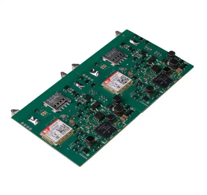
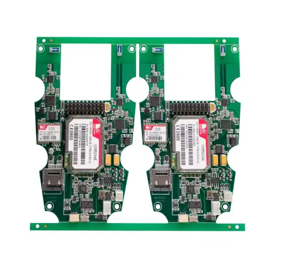
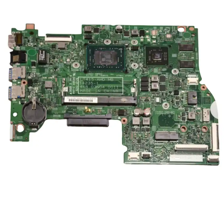
Printed Circuit Board Assembly (PCBA) manufacturing is a sophisticated process that combines cutting-edge technologies with precise engineering to create the backbone of modern electronics. This intricate journey transforms a bare PCB into a fully functional electronic assembly, integrating components through various stages of production. From initial design considerations to final quality control measures, PCBA manufacturing encompasses a range of processes including surface mount technology (SMT), through-hole assembly, and advanced inspection techniques. As industrial PCB assembly continues to evolve, manufacturers are adopting innovative approaches to meet the increasing demands for miniaturization, reliability, and performance in electronic devices across diverse sectors.

The Evolution of PCBA Manufacturing Technologies
From Through-Hole to Surface Mount Technology
The landscape of PCBA manufacturing has undergone a significant transformation over the years. Initially, through-hole technology dominated the industry, where component leads were inserted through holes in the PCB and soldered on the opposite side. While reliable, this method had limitations in terms of board density and automation potential.
The advent of Surface Mount Technology (SMT) revolutionized industrial PCB assembly. SMT allows components to be directly placed and soldered onto the surface of the PCB, enabling higher component density, smaller form factors, and improved electrical performance. This shift has been pivotal in meeting the demands of modern electronics for miniaturization and enhanced functionality.
Advancements in Automated Assembly
Automation has become a cornerstone of PCBA manufacturing, particularly in industrial PCB assembly. Pick-and-place machines, capable of positioning thousands of components per hour with micron-level precision, have dramatically increased production speed and accuracy. These machines use advanced vision systems and algorithms to ensure correct component placement, significantly reducing human error.
Furthermore, the integration of artificial intelligence (AI) and machine learning in PCBA manufacturing has led to more adaptive and efficient production lines. These systems can optimize component placement, predict maintenance needs, and even adjust soldering parameters in real-time based on environmental conditions.
Innovations in Soldering Techniques
Soldering technologies have also seen substantial advancements. Reflow soldering, the primary method for SMT assembly, has been refined with precise temperature profiling and zone control. This ensures optimal solder joint formation across various component types and sizes. For more complex or heat-sensitive components, selective soldering has emerged as a valuable technique in industrial PCB assembly. This method allows for targeted soldering of specific components or areas on the board, minimizing thermal stress on sensitive parts.
Key Processes in Modern PCBA Manufacturing
Design for Manufacturability (DFM)
The PCBA manufacturing process begins long before components are placed on a board. Design for Manufacturability (DFM) is a crucial step where engineers analyze and optimize the PCB design to ensure it can be efficiently and reliably manufactured. This process considers factors such as component spacing, trace widths, and thermal management to prevent issues during assembly and improve overall product quality.
In industrial PCB assembly, DFM is particularly critical due to the often harsh environments and high reliability requirements of industrial electronics. Engineers must consider factors like vibration resistance, thermal cycling, and long-term durability when designing PCBAs for industrial applications.
Solder Paste Application and Component Placement
For SMT assembly, the process typically begins with the application of solder paste to the PCB. This is usually done through a stencil printing process, where a metal stencil with precisely cut apertures is used to deposit solder paste onto the board's solder pads. The accuracy of this step is crucial, as it directly affects the quality of the final solder joints.
Following solder paste application, components are placed onto the board using automated pick-and-place machines. These machines can handle a wide range of component types and sizes, from tiny 0201 resistors to large BGAs (Ball Grid Arrays). The precision and speed of modern placement machines have significantly enhanced the capabilities of industrial PCB assembly.
Reflow Soldering and Inspection
After component placement, the PCB undergoes reflow soldering. In this process, the entire board is heated in a controlled environment, causing the solder paste to melt and form electrical and mechanical connections between the components and the board. Precise temperature control is essential to ensure proper solder joint formation without damaging heat-sensitive components.
Post-reflow inspection is a critical quality control step. Automated Optical Inspection (AOI) systems use high-resolution cameras and sophisticated algorithms to detect defects such as misaligned components, solder bridges, or insufficient solder. For more complex assemblies, especially in industrial PCB assembly, X-ray inspection may be used to examine hidden solder joints beneath BGA components.
Emerging Trends and Future Directions in PCBA Manufacturing
Industry 4.0 and Smart Factories
The concept of Industry 4.0 is reshaping PCBA manufacturing, particularly in the realm of industrial PCB assembly. Smart factories leverage interconnected systems, real-time data analytics, and IoT (Internet of Things) technologies to create more efficient and adaptive production environments. These advancements allow for greater flexibility in production, improved traceability, and enhanced quality control.
In PCBA manufacturing, this translates to production lines that can quickly adapt to different product types, automated material handling systems that ensure continuous component supply, and predictive maintenance systems that minimize downtime. The integration of these technologies is particularly beneficial for industrial PCB assembly, where production runs may be smaller but require higher precision and reliability.
Advanced Materials and Substrate Technologies
As electronic devices become more complex and are required to operate in increasingly challenging environments, new materials and substrate technologies are being developed. High-frequency and high-temperature PCB materials are gaining prominence, especially in industrial and automotive applications where traditional FR-4 substrates may not suffice.
Flexible and rigid-flex PCBs are also becoming more common in industrial PCB assembly. These offer advantages in terms of space-saving, weight reduction, and improved reliability in applications subject to vibration or frequent flexing. The manufacturing processes for these advanced substrates require specialized equipment and expertise, driving innovation in PCBA manufacturing technologies.
Sustainability and Green Manufacturing
Environmental considerations are becoming increasingly important in PCBA manufacturing. The industry is moving towards more sustainable practices, including the use of lead-free solders, reduction of harmful chemicals, and improved energy efficiency in manufacturing processes.
Recycling and circular economy principles are also gaining traction. Manufacturers are developing processes to recover valuable materials from electronic waste, including precious metals from PCB assemblies. This shift towards sustainability is not only environmentally beneficial but also aligns with growing regulatory pressures and consumer expectations for eco-friendly products.
Conclusion
The field of PCBA manufacturing, particularly industrial PCB assembly, is characterized by rapid technological advancement and continuous innovation. From the shift to surface mount technology to the integration of AI and IoT in smart factories, these developments have dramatically enhanced the capabilities, efficiency, and reliability of electronic assemblies. As the industry continues to evolve, addressing challenges such as miniaturization, thermal management, and environmental sustainability will drive further innovations in PCBA manufacturing processes and technologies.
Smart factory with advanced PCBA tech & processes | Ring PCB
Ring PCB offers cutting-edge PCBA solutions with state-of-the-art manufacturing processes. Our advanced technologies ensure high reliability, strong EMI resistance, and wide operating temperature ranges for industrial applications. We provide comprehensive turnkey services, from PCB fabrication to rigorous quality control, optimizing designs for manufacturability and cost-effectiveness. Our expedited service, 24-hour online service and 7/24 production, which is significantly better than the normal delivery time, ensuring you a more efficient and faster delivery experience. For expert PCBA solutions tailored to your needs, contact us at [email protected].
References
1. Zhang, L., & Wang, X. (2019). Advanced Manufacturing Technologies in Printed Circuit Board Assembly: A Comprehensive Review. Journal of Manufacturing Systems, 52, 124-145.
2. Chen, Y., et al. (2020). Industry 4.0 in PCBA Manufacturing: Challenges and Opportunities. IEEE Transactions on Industrial Electronics, 67(9), 7723-7733.
3. Smith, R. J. (2018). Surface Mount Technology: Principles and Practice. Springer Science & Business Media.
4. Johnson, M., & Williams, K. (2021). Sustainable Practices in Electronics Manufacturing: A Focus on PCBA. Environmental Science & Technology, 55(15), 10235-10248.
5. Brown, D. (2022). The Evolution of Industrial PCB Assembly: From Through-Hole to Advanced Packaging Technologies. Industrial Electronics Handbook, 7th Edition, CRC Press.

Welcome to Ring PCB! Share your inquiry, and receive a tailored quotation!

Ring PCB, your trusted partner for PCB & PCBA Full Turnkey Solutions


