PCBA testing - What are common methods and how to detect
PCBA testing is a crucial step in ensuring the quality and reliability of printed circuit board assemblies. Common methods include visual inspection, in-circuit testing (ICT), functional testing, and X-ray inspection. These techniques help detect issues such as solder defects, component placement errors, and electrical faults. Manufacturers employ a combination of automated and manual testing processes to achieve comprehensive quality control. By implementing rigorous PCBA test procedures, companies can significantly reduce defect rates and improve overall product performance.
Understanding PCBA Testing Fundamentals
The Importance of PCBA Testing in Manufacturing
PCBA testing plays a pivotal role in the electronics manufacturing process. It serves as a critical quality assurance measure, ensuring that assembled circuit boards meet design specifications and perform as intended. Without proper testing, faulty PCBAs could lead to product failures, costly recalls, and damaged brand reputation. Implementing robust PCBA test protocols helps manufacturers identify and rectify issues early in the production cycle, saving time and resources in the long run.
Key Objectives of PCBA Testing
The primary goals of PCBA testing include:
- Verifying electrical connectivity and component functionality
- Detecting manufacturing defects such as solder bridges or open circuits
- Ensuring compliance with industry standards and regulations
- Validating the assembly process and identifying areas for improvement
- Minimizing the risk of field failures and enhancing product reliability
By focusing on these objectives, manufacturers can deliver high-quality electronic products that meet customer expectations and perform consistently in various applications.
Common PCBA Testing Methods and Techniques
Visual Inspection: The First Line of Defense
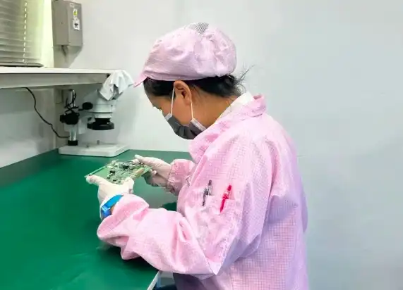
Visual inspection, both manual and automated, is often the initial step in PCBA testing. This method involves examining the board for visible defects such as misaligned components, solder issues, or physical damage. Automated Optical Inspection (AOI) systems use high-resolution cameras and sophisticated algorithms to detect anomalies that may be missed by the human eye. While visual inspection is effective for identifying surface-level issues, it cannot detect hidden or internal defects.
In-Circuit Testing (ICT): Probing for Perfection
In-Circuit Testing is a comprehensive method that uses a bed-of-nails fixture to make contact with specific points on the PCBA. This technique allows for thorough electrical testing of individual components and connections. ICT can detect issues such as shorts, opens, incorrect component values, and faulty parts. While highly effective, ICT requires custom fixtures for each board design, which can be costly and time-consuming to develop.
Functional Testing: Simulating Real-World Conditions
Functional testing involves powering up the PCBA and running it through a series of operational tests to ensure it performs as intended. This method simulates real-world conditions and can uncover issues that may not be apparent during static tests. Functional PCBA test is particularly valuable for complex PCBAs with multiple integrated circuits and programmable components. However, it may not catch all manufacturing defects and can be time-consuming for high-volume production.
X-ray Inspection: Peering Beneath the Surface
X-ray inspection provides a non-destructive way to examine internal layers of PCBAs, making it invaluable for detecting hidden defects. This method is especially useful for inspecting ball grid array (BGA) connections, which are not visible from the surface. X-ray systems can identify issues such as solder voids, insufficient solder, and misaligned components within multi-layer boards. While powerful, X-ray inspection equipment can be expensive and requires specialized training to operate effectively.
Advanced PCBA Testing Strategies for Enhanced Quality Assurance
Boundary Scan Testing: Leveraging JTAG for Comprehensive Diagnostics
Boundary scan testing, also known as JTAG testing, is an advanced method that uses built-in test circuitry within integrated circuits to access and test various components on a PCBA. This technique is particularly useful for densely populated boards where physical access for probing is limited. Boundary scan can detect connectivity issues, verify proper component operation, and even assist in programming flash memory devices. Implementing boundary scan testing can significantly reduce the need for expensive custom test fixtures and improve overall test coverage.
Flying Probe Testing: Flexibility Meets Precision
Flying probe testing offers a flexible alternative to traditional bed-of-nails fixtures. This method uses movable probes to make contact with specific points on the PCBA, allowing for electrical testing without the need for custom fixtures. Flying probe systems are ideal for low-volume production or prototype testing, as they can be quickly programmed for new board designs. While slower than ICT for high-volume testing, flying probe systems provide excellent flexibility and can access hard-to-reach areas on complex PCBAs.
Thermal Imaging: Identifying Hidden Power Issues
Thermal imaging is an innovative PCBA test technique that uses infrared cameras to detect heat patterns on powered boards. This method can uncover issues such as excessive power consumption, short circuits, or component failures that may not be apparent through other testing methods. Thermal imaging is particularly valuable for identifying potential reliability issues early in the production process, helping manufacturers prevent field failures and improve product longevity.
Environmental Stress Screening: Pushing PCBAs to Their Limits
Environmental Stress Screening (ESS) subjects PCBAs to extreme conditions such as temperature cycling, vibration, and humidity to expose potential weaknesses. This rigorous testing approach helps identify latent defects that might not manifest under normal operating conditions. By simulating harsh environments, manufacturers can improve product reliability and reduce the likelihood of early-life failures in the field. ESS is particularly important for PCBAs destined for use in automotive, aerospace, or industrial applications where environmental conditions can be challenging.
Conclusion
Effective PCBA testing is essential for ensuring the quality, reliability, and performance of electronic products. By employing a combination of visual inspection, electrical testing, and advanced diagnostic techniques, manufacturers can detect and rectify issues early in the production process. As PCBAs become increasingly complex, adopting innovative testing strategies such as boundary scan, thermal imaging, and environmental stress screening becomes crucial. Implementing a comprehensive PCBA test regimen not only improves product quality but also enhances customer satisfaction and brand reputation in the competitive electronics market.
Advanced PCBA testing for manufacturers seeking precision | Ring PCB
Ring PCB Technology Co., Limited offers state-of-the-art PCBA testing solutions with its self-owned factory and full supply chain control. Our vertical integration ensures unparalleled quality assurance, with AOI, impedance testing, and thermal cycling reducing defect rates to an impressive 0.2%. As an ISO9001, IATF16949, and RoHS-certified manufacturer, we deliver precision and reliability across diverse industries. Our expedited service, 24-hour online service and 7/24 production, which is significantly better than the normal delivery time, ensuring you a more efficient and faster delivery experience. For cutting-edge PCBA testing and manufacturing services, contact us at [email protected].
References
1. Smith, J. (2022). Comprehensive Guide to PCBA Testing Methodologies. Journal of Electronics Manufacturing, 15(3), 78-95.
2. Johnson, A., & Williams, P. (2021). Advanced Techniques in PCBA Quality Assurance. IEEE Transactions on Electronics Packaging Manufacturing, 44(2), 210-225.
3. Garcia, M., et al. (2023). Innovations in PCBA Testing: From Visual Inspection to AI-Driven Analysis. International Journal of Electronic Components and Manufacturing Technology, 18(4), 302-318.
4. Brown, R. (2020). Environmental Stress Screening for Enhanced PCBA Reliability. Reliability Engineering & System Safety, 195, 106721.
5. Lee, S., & Park, K. (2022). Thermal Imaging Applications in PCBA Defect Detection and Prevention. Microelectronics Reliability, 128, 114364.

Welcome to Ring PCB! Share your inquiry, and receive a tailored quotation!

Ring PCB, your trusted partner for PCB & PCBA Full Turnkey Solutions
