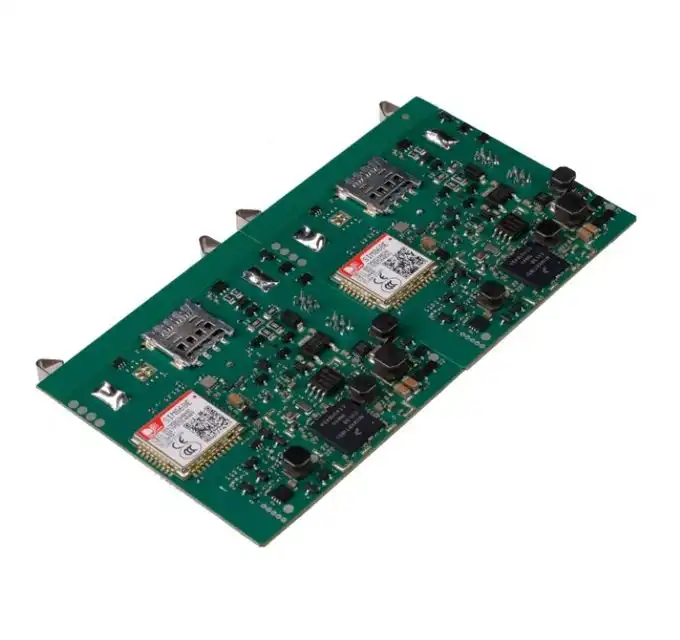
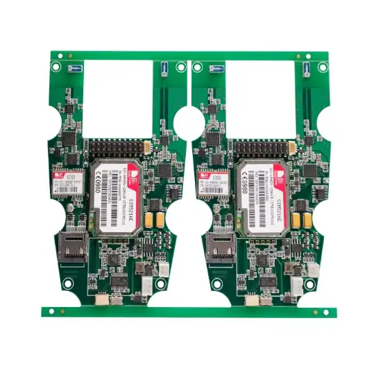
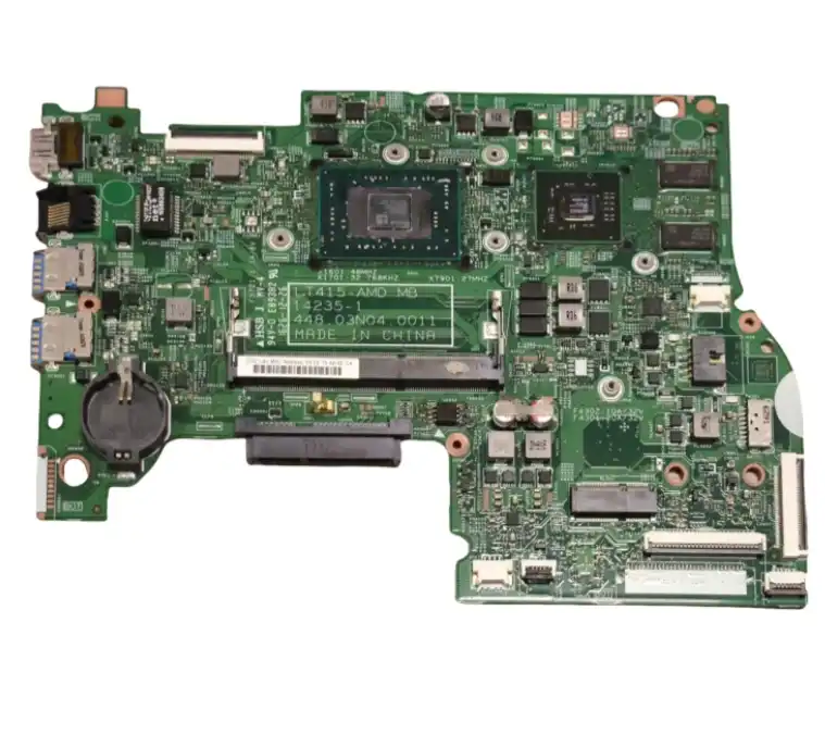
Printed Circuit Boards Assembly (PCBA) Process
The Printed Circuit Boards Assembly (PCBA) process is a sophisticated manufacturing procedure that transforms bare printed circuit boards (PCBs) into fully functional electronic assemblies. This intricate process involves mounting various electronic components onto the PCB, creating a complete circuit ready for integration into electronic devices. PCB assembly is a critical step in electronics manufacturing, combining precision engineering, advanced technology, and meticulous quality control to produce reliable and efficient electronic products. From smartphones to automotive systems, the PCBA process plays a pivotal role in bringing modern electronics to life.
Understanding the Fundamentals of PCB Assembly
What is PCB Assembly?
PCB assembly refers to the process of soldering electronic components onto a printed circuit board. This crucial step transforms a bare PCB into a functional electronic circuit. The assembly process involves several stages, each contributing to the final product's quality and performance.
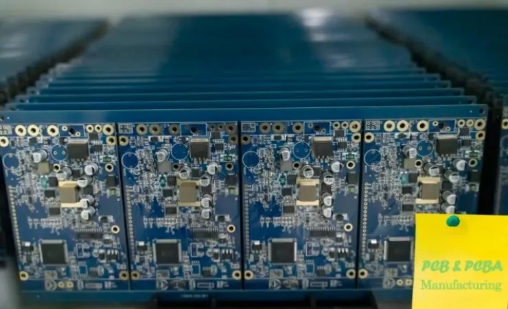
Types of PCB Assembly
There are two primary types of PCB assembly: Surface Mount Technology (SMT) and Through-Hole Technology (THT). SMT involves mounting components directly onto the surface of the PCB, while THT requires components to be inserted through holes in the board. Many modern assemblies use a combination of both techniques to optimize performance and space utilization.
Key Components in PCB Assembly
A typical PCB assembly includes various electronic components such as resistors, capacitors, integrated circuits (ICs), connectors, and more. The selection and placement of these components are crucial for the circuit's functionality. Advanced assemblies may also incorporate specialized components like microprocessors, sensors, or power management modules.
The Step-by-Step PCB Assembly Process
Solder Paste Application
The PCBA process begins with applying solder paste to the bare PCB. This paste, a mixture of tiny solder particles and flux, is precisely deposited onto the board's solder pads using a stencil and a paste-printing machine. The accuracy of this step is critical as it determines the quality of component attachment.
Component Placement
Following solder paste application, components are placed onto the board using automated pick-and-place machines. These high-speed robots can accurately position thousands of components per hour, ensuring precise alignment with the solder paste deposits. For more complex or delicate components, manual placement may be necessary.
Reflow Soldering
Once components are placed, the PCB undergoes reflow soldering. In this process, the board is heated in a reflow oven, melting the solder paste and creating permanent connections between components and the PCB. The temperature profile is carefully controlled to ensure proper soldering without damaging sensitive components.
Inspection and Quality Control
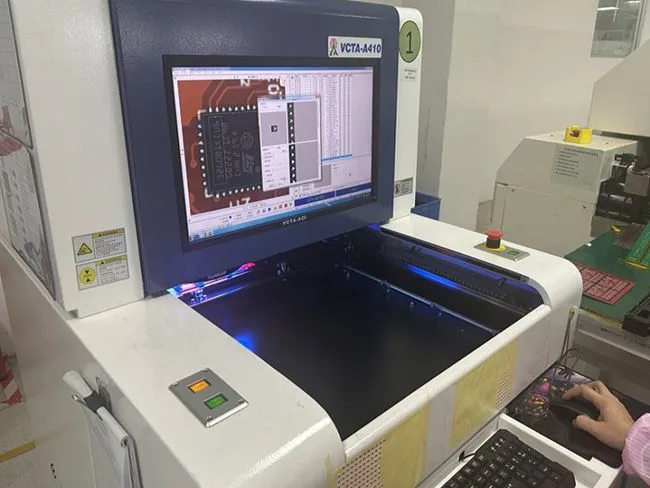
After reflow, the assembled PCB undergoes rigorous inspection. Automated Optical Inspection (AOI) systems scan the board for defects such as misaligned components or solder bridges. X-ray inspection may be used for complex multi-layer boards or Ball Grid Array (BGA) components. Any identified issues are addressed through rework or repair processes.
Through-Hole Component Insertion
For boards requiring through-hole components, these are inserted either manually or by automated insertion machines. This step often follows the SMT process and requires careful handling to avoid damaging previously placed surface-mount components.
Wave Soldering
Through-hole components are typically soldered using wave soldering. The PCB is passed over a wave of molten solder, which adheres to the exposed metal parts, creating secure connections. This process requires precise control of solder temperature and wave height to ensure quality connections without damaging components.
Final Inspection and Functional Testing
The fully assembled PCB undergoes a final inspection and functional testing. This may include visual inspections, in-circuit testing to verify component values and connections, and functional tests to ensure the board operates as intended. Any boards failing these tests are either reworked or scrapped, depending on the nature of the defect.
Advanced Technologies and Trends in PCB Assembly
Automation and Industry 4.0
The PCB assembly industry is increasingly adopting automation and Industry 4.0 principles. Smart factories utilize interconnected systems, real-time data analytics, and machine learning to optimize production processes, improve quality control, and increase efficiency. Automated guided vehicles (AGVs) and collaborative robots are becoming common in assembly lines, enhancing productivity and reducing human error.
Miniaturization and High-Density Interconnect (HDI) PCBs
As electronic devices become smaller and more powerful, PCB assembly techniques are evolving to accommodate miniaturization trends. High-Density Interconnect (HDI) PCBs, featuring finer lines and spaces, smaller vias, and higher connection pad density, require advanced assembly techniques. Micro Ball Grid Array (μBGA) and Chip Scale Package (CSP) technologies are increasingly used to maximize component density on these compact boards.
Environmentally Friendly Practices
The PCB assembly industry is adopting more environmentally friendly practices in response to global sustainability initiatives. This includes the use of lead-free solders, implementing energy-efficient manufacturing processes, and developing recycling programs for electronic waste. Water-soluble flux technologies are also gaining popularity, reducing the need for harsh cleaning chemicals in the assembly process.
3D Printing in PCB Assembly
3D printing technology is making inroads in PCB assembly, particularly for prototyping and small-scale production. Additive manufacturing techniques allow for rapid production of custom PCB designs, including multi-layer boards and flexible circuits. While still in its early stages, 3D-printed electronics hold promise for reducing time-to-market and enabling more complex, customized designs.
Conclusion
The PCB assembly process is a complex and critical aspect of electronics manufacturing. From the initial application of solder paste to the final quality control checks, each step in the PCBA process contributes to the reliability and performance of the finished electronic product. As technology continues to advance, PCB assembly techniques evolve to meet the demands of miniaturization, increased functionality, and environmental sustainability. Understanding this process is essential for anyone involved in electronics design, manufacturing, or quality assurance, as it forms the backbone of our modern electronic world.
Precision-driven PCBA process with zero-defect delivery | Ring PCB
Ring PCB, your trusted PCB Manufacturing Partner since 2008, offers a precision-driven PCBA process aimed at zero-defect delivery. Our self-owned factory ensures full supply chain control through vertical integration, managing raw material procurement, production, and testing in-house. We implement a Triple Quality Assurance system, combining AOI, impedance testing, and thermal cycling, achieving an industry-leading defect rate of <0.2%.
Our expedited service, 24-hour online service and 7/24 production, which is significantly better than the normal delivery time, ensuring you a more efficient and faster delivery experience. With global certifications including ISO9001, IATF16949, and RoHS compliance, we guarantee top-quality PCB assembly services. For more information, contact us at [email protected].
References
1. Coombs, C. F. (2008). Printed Circuits Handbook. McGraw-Hill Professional.
2. Prasad, R. P. (1997). Surface Mount Technology: Principles and Practice. Springer Science & Business Media.
3. Hwang, J. S. (2005). Environment-Friendly Electronics: Lead-Free Technology. Electrochemical Publications.
4. Scheller, B. (2019). Manufacturing Techniques for Printed Circuit Boards. CRC Press.
5. Lau, J. H. (2016). 3D IC Integration and Packaging. McGraw Hill Professional.

Welcome to Ring PCB! Share your inquiry, and receive a tailored quotation!

Ring PCB, your trusted partner for PCB & PCBA Full Turnkey Solutions
