The Importance of Advanced PCBA Testing in Modern Electronics Manufacturing
In today's rapidly evolving electronics landscape, the complexity of printed circuit board assemblies (PCBAs) continues to increase. This complexity, coupled with the demand for higher reliability and performance, necessitates sophisticated testing methodologies. Advanced PCBA Testing Solutions play a crucial role in ensuring the quality and functionality of electronic products across various industries, from consumer electronics to automotive and aerospace applications.
These testing solutions go beyond simple continuity checks, employing a multi-faceted approach to detect potential issues. By utilizing a combination of visual, electrical, and functional tests, manufacturers can identify defects ranging from solder joint problems to component malfunctions. This comprehensive testing strategy is particularly vital for high-density interconnect (HDI) and multilayer PCBs, where traditional inspection methods may fall short.
Moreover, advanced PCBA Testing Solutions contribute significantly to the overall efficiency of the manufacturing process. By detecting issues early in the production cycle, manufacturers can avoid costly rework and reduce time-to-market. This proactive approach not only saves resources but also enhances the reputation of the manufacturer by ensuring consistent product quality.
Automated Optical Inspection (AOI) in PCBA Testing
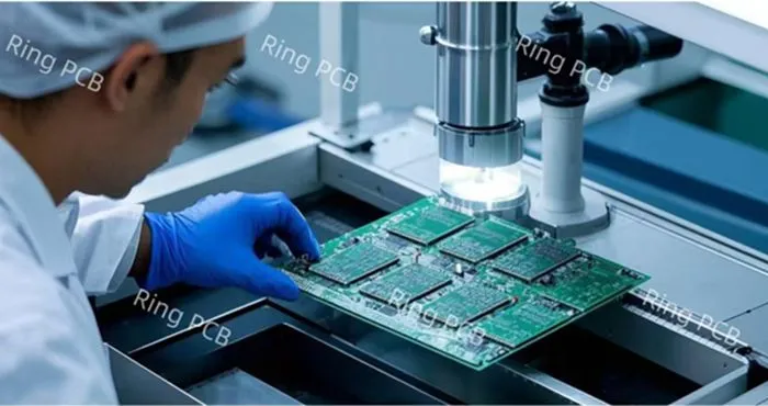
Automated Optical Inspection (AOI) is a cornerstone of modern PCBA Testing Solutions. This non-contact inspection method uses high-resolution cameras and sophisticated image processing algorithms to detect visual defects on assembled PCBs. AOI systems can identify issues such as missing components, incorrect component placement, solder bridging, and other surface-level anomalies.
The advantages of AOI in PCBA testing are numerous. It offers high-speed inspection capabilities, allowing for 100% inspection of boards in a production line without slowing down the manufacturing process. AOI systems can also be programmed to detect subtle defects that might be missed by human inspectors, ensuring consistency and reliability in the inspection process.
Furthermore, AOI technology has evolved to handle increasingly complex PCB designs. Advanced systems can now inspect fine-pitch components, ball grid arrays (BGAs), and other challenging features commonly found in modern electronics. This capability is particularly valuable for manufacturers dealing with high-density PCBAs used in cutting-edge applications.
X-ray Inspection: Unveiling Hidden Defects in Complex PCB Assemblies
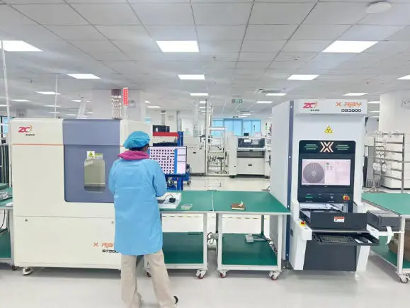
X-ray inspection has become an indispensable tool in comprehensive PCBA Testing Solutions, especially for complex multilayer and high-density interconnect (HDI) boards. Unlike optical inspection methods, X-ray systems can penetrate through the layers of a PCB, revealing hidden defects that would otherwise go undetected.
This non-destructive testing technique is particularly effective in inspecting ball grid array (BGA) components, where solder joints are concealed beneath the package. X-ray inspection can identify issues such as voids in solder joints, misaligned components, and internal short circuits. For high-reliability applications, such as automotive and aerospace electronics, X-ray inspection is often mandatory to ensure the integrity of critical connections.
Advanced X-ray systems used in PCBA Testing Solutions offer features like 3D imaging and tomography, providing detailed insights into the internal structure of PCB assemblies. These capabilities allow manufacturers to perform in-depth analysis of solder joint quality, component placement accuracy, and overall board integrity. By leveraging X-ray inspection, manufacturers can significantly reduce the risk of latent defects and improve the long-term reliability of their products.
In-Circuit Testing (ICT) for Comprehensive Electrical Verification
In-Circuit Testing (ICT) is a crucial component of advanced PCBA Testing Solutions, providing thorough electrical verification of assembled circuit boards. ICT systems use a bed-of-nails fixture to make contact with specific points on the PCB, allowing for rapid and accurate testing of individual components and circuit paths.
The primary advantage of ICT is its ability to detect a wide range of electrical defects, including short circuits, open circuits, incorrect component values, and faulty components. This testing method is particularly effective in identifying manufacturing defects such as missing or wrong components, poor solder joints, and incorrect assembly.
Modern ICT systems have evolved to handle the challenges posed by high-density PCBAs. Advanced fixtures and test algorithms enable testing of fine-pitch components and densely populated boards. Additionally, many ICT systems now incorporate boundary scan testing capabilities, allowing for improved test coverage on boards with limited physical access points.
Functional Testing: Ensuring Real-World Performance of PCB Assemblies
While visual and electrical tests are essential, functional testing remains a critical aspect of comprehensive PCBA Testing Solutions. Functional testing simulates real-world operating conditions to verify that the assembled PCB performs as intended in its final application. This type of testing is crucial for detecting issues that may not be apparent through other testing methods.
Functional testing can range from simple power-up tests to complex simulations of the product's intended use environment. For instance, in automotive electronics, functional tests might include temperature cycling, vibration testing, and electromagnetic compatibility (EMC) checks. These tests ensure that the PCBA can withstand the rigors of its intended operating environment.
Advanced functional testing setups often incorporate automated test equipment (ATE) that can rapidly cycle through various test scenarios. This automation not only increases testing speed and consistency but also allows for the collection of valuable data that can be used for process improvement and quality control.
Integrating AI and Machine Learning in PCBA Testing
The integration of artificial intelligence (AI) and machine learning (ML) technologies is revolutionizing PCBA Testing Solutions. These advanced technologies are enhancing the capabilities of traditional testing methods, making them more efficient and effective.
In AOI systems, AI algorithms can improve defect detection accuracy by learning from historical data and adapting to new types of defects. This capability is particularly valuable in high-mix, low-volume production environments where traditional rule-based inspection might struggle.
Machine learning is also being applied to analyze data from various testing stages, including ICT and functional testing. By processing vast amounts of test data, ML algorithms can identify subtle patterns and correlations that might indicate potential quality issues or predict future failures. This predictive capability allows manufacturers to take proactive measures to improve product reliability and manufacturing processes.
Conclusion
Comprehensive PCBA Testing Solutions are indispensable in today's electronics manufacturing landscape. By combining advanced technologies such as AOI, X-ray inspection, ICT, and functional testing, manufacturers can significantly reduce product failures and enhance overall quality. The integration of AI and machine learning further augments these capabilities, paving the way for even more sophisticated and effective testing methodologies.
For companies seeking to optimize their PCB assembly processes and minimize product failures, partnering with experienced PCBA Testing Solutions providers is crucial. These suppliers and manufacturers offer the expertise and advanced equipment necessary to implement robust testing strategies tailored to specific product requirements. By leveraging comprehensive testing solutions, electronics manufacturers can ensure the reliability and performance of their products in an increasingly competitive market.
FAQ
What are the key benefits of implementing comprehensive PCBA Testing Solutions?
Comprehensive PCBA Testing Solutions offer numerous benefits, including improved product reliability, reduced warranty claims, faster time-to-market, and enhanced manufacturing efficiency. These solutions help identify and rectify defects early in the production process, ensuring high-quality electronic assemblies.
How does X-ray inspection contribute to PCBA testing?
X-ray inspection allows for non-destructive examination of internal PCB structures, making it invaluable for inspecting hidden solder joints, BGA components, and multilayer boards. It helps detect issues like voids, misalignments, and internal defects that are not visible through optical inspection methods.
Can PCBA Testing Solutions handle high-density and complex PCB designs?
Yes, advanced PCBA Testing Solutions are designed to handle high-density interconnect (HDI) and complex multilayer PCBs. They employ sophisticated technologies like high-resolution AOI, 3D X-ray imaging, and advanced ICT fixtures to ensure thorough testing of even the most complex PCB assemblies.
Comprehensive PCBA Services: From Design to Delivery | Ring PCB
Ring PCB offers end-to-end PCBA services, combining cutting-edge manufacturing with rigorous testing solutions. Our expertise spans from rapid prototyping to high-volume production, catering to diverse industries. We provide DFM optimization, component sourcing, SMT assembly, and comprehensive testing including AOI, X-ray, and functional validation. For quality-driven, cost-effective PCBA solutions, contact us at [email protected].
References
1. Johnson, A. (2022). "Advanced PCBA Testing Methodologies for Reducing Product Failures." Journal of Electronics Manufacturing, 15(3), 78-92.
2. Smith, R. & Brown, T. (2021). "The Role of AI in Enhancing PCBA Testing Accuracy." IEEE Transactions on Industrial Electronics, 68(9), 8765-8779.
3. Lee, S. et al. (2023). "Comprehensive Analysis of X-ray Inspection Techniques in Modern PCBA Testing." International Journal of Production Research, 61(4), 1235-1250.
4. Garcia, M. (2022). "Functional Testing Strategies for High-Reliability PCB Assemblies." Quality and Reliability Engineering International, 38(2), 567-582.
5. Thompson, E. & Wilson, K. (2023). "Integration of Machine Learning in PCBA Defect Detection and Classification." IEEE Access, 11, 45678-45692.
