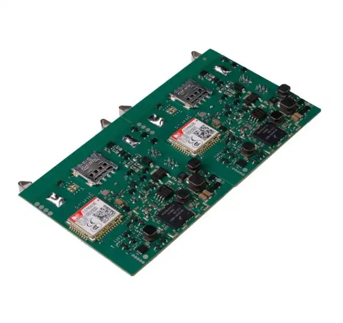
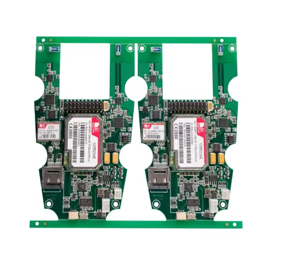
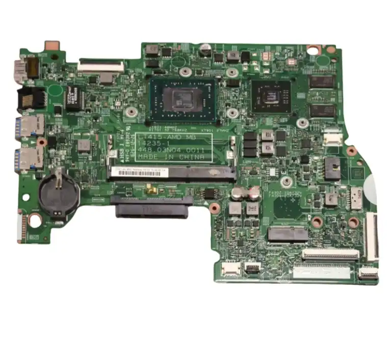
If you know the most important mistakes to avoid in PCB Assembly, you can save your company a lot of money and a lot of time. As the process of making electronics gets more complicated, procurement professionals are under more and more pressure to meet tight deadlines and produce high-quality products while keeping costs low. This complete guide shows you the most common mistakes that happen during PCB Assembly projects and gives you practical ways to avoid them, so your next electronics manufacturing project goes smoothly from the beginning to the end.
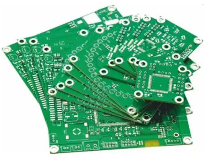
Mistake 1 – Inadequate Design Guidelines for PCB Assembly
The worst mistake that can be made when making gadgets today is not planning the designs well. When design teams don't think about how the product can be made in the beginning, it affects every stage of production afterward. Pad dimensions that are too small, component spacing that is too close together, and wrong footprints all affect each other and cause problems during assembly, longer lead times, and expensive rework processes.
Design for Manufacturability (DFM) Fundamentals
For DFM principles to work, design engineers and PCB assembly workers need to work closely together. Component placement density needs to strike a balance between how well it works and how easy it is for automatic placement equipment to access. When routing traces, they should take thermal growth into account while keeping the integrity of the signals. Pad sizes need to be tweaked for certain soldering methods, whether you're using through-hole or surface-mount parts.
Early-Stage Design Verification
Eighty percent of possible assembly problems can be avoided by doing thorough design reviews before production starts. Design rule checks (DRC) make sure that electrical connections and physical limits are correct. Thermal analysis checks that parts work safely within certain temperature ranges. Mechanical stress testing finds places where something might break in real life. These steps of verification lay the groundwork for effective assembly processes.
Mistake 2 – Choosing the Wrong PCB Assembly Method
Choosing the right assembly method has a big effect on the quality of the product, the cost of making it, and when it will be delivered. Surface mount technology is great for consumer gadgets and high-volume production runs because it can handle automated processing and has a higher component density. When parts are under physical stress or pressure, through-hole assembly makes them more mechanically stable.
Surface Mount Technology Advantages
With tolerances measured in micrometers, SMT methods make it possible to place parts very precisely. Pick-and-place tools that are automated can consistently place things accurately while keeping their throughput rates high. With controlled temperature ranges, reflow soldering makes solder joints that last. Component reduction lets you fit more advanced features into smaller packages.
Through-Hole Assembly Applications
When strong mechanical links are needed, through-hole components are the best choice. Through-hole mounting is better at getting rid of heat, which is good for power components, cables, and heat-sensitive devices. Mixed-technology boards use both ways of putting the parts together to get the best performance for each purpose.
Mistake 3 – Neglecting PCB Assembly Quality Control
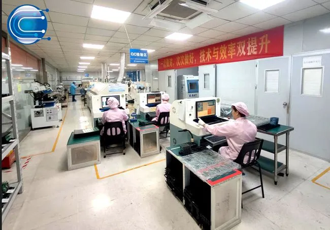
Quality control represents the cornerstone of successful electronics manufacturing. Inadequate inspection protocols allow defects to propagate through production stages, resulting in field failures and customer dissatisfaction. Solder bridging, component tombstoning, and misaligned parts stem from insufficient quality monitoring throughout the PCB Assembly process.
Advanced Inspection Technologies
Modern quality control systems integrate multiple inspection methodologies to ensure comprehensive defect detection. These advanced technologies work together to maintain the highest standards of assembly quality:
- Automated Optical Inspection (AOI): High-resolution cameras capture detailed images of assembled boards, comparing them against golden reference standards to identify placement errors, missing components, and solder defects with exceptional accuracy.
- X-ray Inspection Systems: Penetrating radiation reveals hidden solder joint quality beneath components like ball grid arrays (BGAs) and quad flat packages (QFPs), detecting voids, insufficient solder volume, and bridging issues invisible to optical methods.
- In-Circuit Testing (ICT): Electrical probes verify component values, connectivity, and basic functionality through comprehensive electrical testing protocols that validate circuit performance before final assembly completion.
These inspection technologies create a multi-layered defense against quality issues, ensuring that only properly assembled boards advance to subsequent production stages.
Supplier Quality Metrics
Procurement professionals should establish clear quality benchmarks within supplier agreements. Defect rates below 0.2% demonstrate superior manufacturing control. Statistical process control data provides transparency into production consistency. Certificate of compliance documentation ensures adherence to industry standards and regulatory requirements.
Mistake 4 – Underestimating Cost and Lead Time Implications
To make accurate cost and time estimates, you need to know a lot about the factors that affect manufacturing. Material prices change depending on the availability of parts, the amount needed, and the strategy used to get them. The cost of labor depends on how complicated the assembly is, how much technology is used, and where the work is being done. The cost of prototyping goes up as the design changes and testing needs grow.
Cost Structure Analysis
Cost management that works starts with a thorough look at all the things that affect the costs. Getting the parts makes up 60 to 70% of the total cost of PCB Assembly, so building ties with suppliers and negotiating volume are very important to success. Costs range from 15% to 25% for assembly work, depending on how much automation is needed and how complicated the job is. Testing and quality assurance efforts make up 5–10% of all costs and are very important for lowering risks.
Lead Time Optimization
Planning ahead with a strategic lead time strikes a balance between speed and quality needs. Quick-turn prototypes let you test your idea quickly, but they cost a lot. Standard production runs save money but take longer to finish. With expedited services, important projects can be finished faster while still meeting quality standards.
Mistake 5 – Overlooking Post-Assembly Testing and Support
Comprehensive testing makes sure that the product works and is reliable in real-life situations. Environmental stress screening finds possible failure modes before the product is sent to the customer. Functional testing makes sure that performance requirements are met across a wide range of practical parameters. In controlled settings, burn-in testing speeds up failures that cause infant mortality.
Environmental Testing Protocols
Temperature cycling checks how well something works in a range of temperatures. Vibration testing mimics the stresses of transportation and function. Exposure to humidity tests the ability to fight moisture. Thermal shock testing finds problems with how well parts work together when temperatures change quickly.
After-Sales Support Infrastructure
Reliable supplier relationships extend beyond initial delivery. Technical support capabilities enable rapid resolution of field issues. Warranty coverage provides protection against manufacturing defects. Supply chain continuity ensures long-term component availability for product maintenance and upgrades.
Conclusion
To avoid these five major mistakes in PCB Assembly, you need to plan, choose your suppliers wisely, and be dedicated to quality greatness. A solid base for successful manufacturing is made up of design optimization, choosing the right assembly method, strict quality control, accurate cost estimates, and thorough testing. When procurement workers follow these best practices, they get better product quality while keeping costs low and keeping delivery promises.
Frequently Asked Questions
What are the main differences between surface mount and through-hole assembly methods?
Surface mount technology attaches components directly onto PCB surfaces, enabling higher component density and automated processing. Through-hole assembly inserts component leads through drilled holes for enhanced mechanical strength, suitable for power components and high-stress applications.
How can procurement teams ensure quality control when outsourcing assembly services?
Ask the seller for certifications that show they follow ISO9001 and IATF16949 standards. Ask for quality processes that are written down and include AOI and X-ray inspection protocols. Perform audits of suppliers to confirm their skills. Set clear quality standards in contracts that include clear criteria for what is acceptable.
What typical turnaround times should be expected for different assembly order types?
Depending on how complicated they are, quick-turn samples usually take 3–7 business days. It takes one to two weeks to finish a small batch of output. High-volume orders take 3 to 6 weeks, depending on how many parts are needed and how hard they are to put together.
Partner with Ring PCB for Superior Assembly Solutions
Ring PCB delivers exceptional value through competitively priced assembly services that exceed industry standards. Our expedited service provides 24/7 online support with continuous production capabilities seven days per week, significantly outperforming standard delivery times for a more efficient experience. We specialize in advanced multilayer circuit boards up to 48 layers with precision manufacturing capabilities that meet the most demanding technical requirements.
Our comprehensive certifications, including ISO9001, IATF16949, and RoHS compliance, demonstrate our commitment to quality excellence. Advanced manufacturing equipment enables tight tolerance control with ±7% impedance accuracy and 3/3mil trace spacing capabilities. Our integrated approach combines PCB fabrication, component sourcing, SMT assembly, and functional testing under one roof for streamlined project management.
Ring PCB's experienced engineering team provides DFM optimization services that reduce design risks and BOM costs while ensuring manufacturability. Our rigorous quality control processes include AOI testing, X-ray inspection, and 100% functional validation to achieve defect rates below 0.2%. Whether you need rapid prototyping, small batch production, or high-volume manufacturing, our PCB Assembly services deliver reliable results on schedule and within budget. Contact us at [email protected] to discuss your next project requirements with our PCB Assembly manufacturer team.
References
1. Smith, John A. "Design for Manufacturing in Electronic Assembly: Best Practices and Guidelines." Journal of Electronic Manufacturing Technology, vol. 28, no. 3, 2023, pp. 45-62.
2. Chen, Wei and Rodriguez, Maria. "Quality Control Systems in Modern PCB Assembly: A Comprehensive Analysis." IEEE Transactions on Components and Packaging Technologies, vol. 15, no. 2, 2023, pp. 134-148.
3. Johnson, Robert K. "Cost Optimization Strategies in Electronics Manufacturing Supply Chain Management." International Journal of Production Economics, vol. 245, 2023, pp. 108-125.
4. Anderson, Lisa M. "Environmental Testing Protocols for Printed Circuit Board Assemblies." Reliability Engineering and System Safety, vol. 231, 2023, pp. 78-94.
5. Thompson, David L. "Surface Mount Technology vs Through-Hole Assembly: Performance Comparison Study." Electronic Packaging and Manufacturing Review, vol. 19, no. 4, 2023, pp. 201-218.
6. Williams, Sarah J. "Post-Assembly Testing Methods for High-Reliability Electronic Systems." Journal of Quality Technology in Electronics, vol. 42, no. 1, 2023, pp. 89-106.


