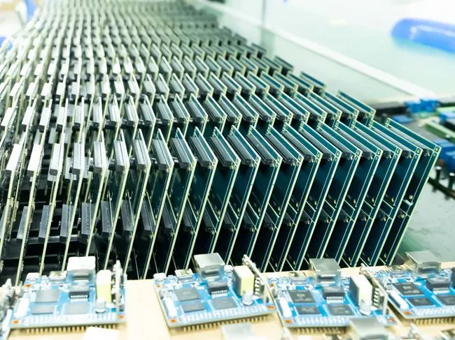
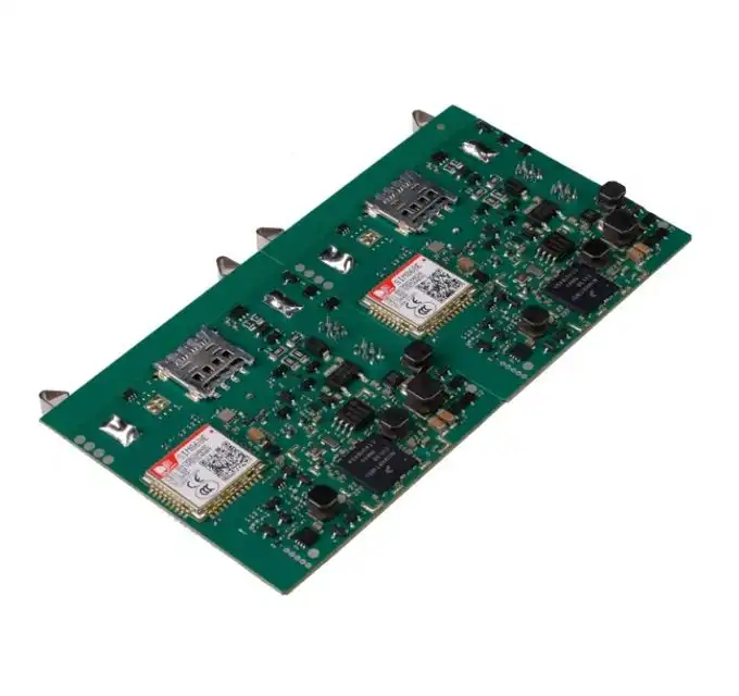
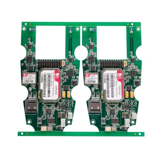
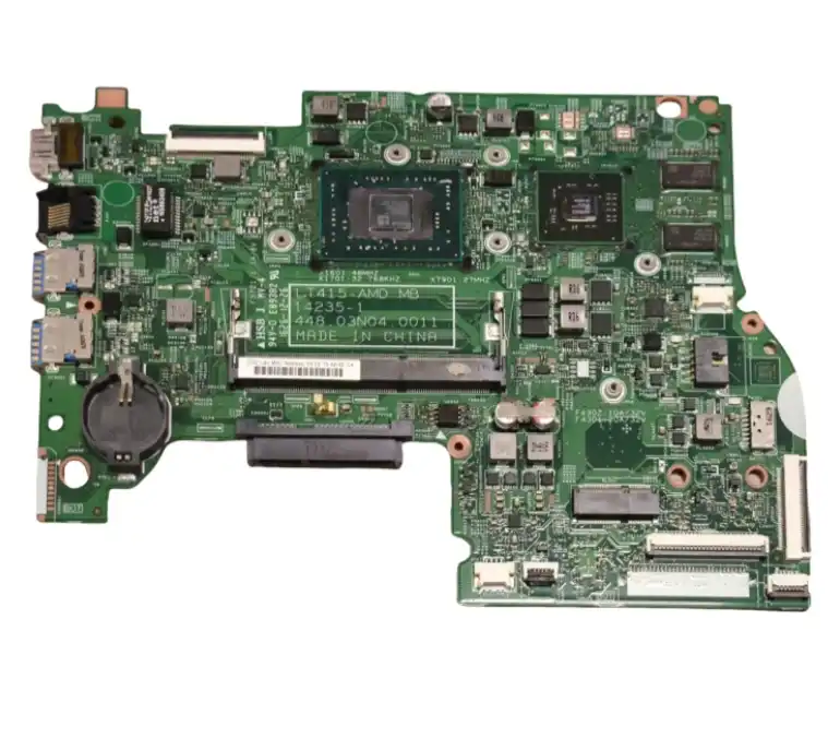
The Evolution and Impact of PCB SMT in Electronics Manufacturing
The journey of PCB SMT began in the 1960s, but it wasn't until the 1980s that it gained significant traction in the electronics industry. This technological leap marked a paradigm shift from traditional through-hole technology, where component leads were inserted through holes in the circuit board. SMT's adoption was driven by the increasing demand for miniaturization and improved performance in electronic devices.
One of the most significant advantages of PCB SMT is its ability to dramatically reduce the size of electronic components and the overall footprint of circuit boards. This miniaturization has paved the way for the development of ultra-compact devices like smartphones, wearables, and IoT devices. The reduced size not only makes devices more portable but also allows for the integration of more features and functionalities within the same space.
Efficiency and Performance Enhancements
PCB SMT doesn't just shrink device size; it also enhances performance. Surface-mounted components have shorter lead lengths, which reduces parasitic capacitance and inductance. This reduction in electrical noise and signal distortion results in improved high-frequency performance, crucial for modern high-speed digital circuits and wireless communication devices.
Moreover, SMT allows for higher component density on PCBs. This increased density translates to shorter signal paths, which in turn leads to faster processing speeds and reduced power consumption. These improvements are particularly valuable in applications where energy efficiency and processing power are paramount, such as in mobile devices and data centers.
Manufacturing Advancements and Cost Reduction
The adoption of PCB SMT has revolutionized the manufacturing process of electronic devices. Automated pick-and-place machines can rapidly and accurately place thousands of components per hour, significantly increasing production efficiency. This automation not only speeds up the manufacturing process but also reduces human error, leading to higher product quality and consistency.
From a cost perspective, SMT offers several advantages. The reduced size of components and boards means less material usage, translating to lower raw material costs. The automated assembly process reduces labor costs and increases throughput, further driving down production expenses. Additionally, the improved reliability of SMT-assembled devices leads to fewer warranty claims and repairs, contributing to overall cost savings for manufacturers and consumers alike.
Key Components and Processes in PCB SMT Assembly
Understanding the components and processes involved in PCB SMT assembly is crucial for appreciating its role in modern electronics. The assembly process is a carefully orchestrated sequence of steps, each critical to the final product's quality and functionality.
Surface Mount Components
At the heart of SMT are the surface mount components themselves. These come in various forms, each designed for specific applications:
- Resistors and Capacitors: Often in chip form, these passive components are significantly smaller than their through-hole counterparts.
- Integrated Circuits (ICs): Available in various package types like QFP (Quad Flat Package), BGA (Ball Grid Array), and CSP (Chip Scale Package), allowing for complex functionality in compact forms.
- LEDs and Diodes: Surface mount versions of these components enable the creation of thin, flexible displays and efficient lighting solutions.
- Connectors: SMT connectors save board space and offer improved high-frequency performance.
The SMT Assembly Process
The PCB SMT assembly process typically involves the following steps:
- Solder Paste Application: A precise amount of solder paste is applied to the PCB using a stencil and squeegee or a jet printer.
- Component Placement: Advanced pick-and-place machines accurately position components onto the solder paste.
- Reflow Soldering: The board passes through a reflow oven where the solder paste melts, forming electrical and mechanical connections.
- Inspection and Testing: Automated optical inspection (AOI) and X-ray inspection ensure proper component placement and solder joint quality.
- Additional Processes: For double-sided boards or mixed-technology assemblies, additional steps like wave soldering or manual soldering might be employed.
This streamlined process allows for high-volume production of complex electronic assemblies with exceptional precision and reliability.
Challenges and Future Trends in PCB SMT Technology
While PCB SMT has revolutionized electronics manufacturing, it also presents unique challenges and continues to evolve to meet future demands.
Current Challenges in PCB SMT
Some of the primary challenges faced in PCB SMT include:
- Component Miniaturization: As components become smaller, placing and soldering them accurately becomes more challenging, requiring more advanced equipment and techniques.
- Heat Management: Increased component density can lead to heat dissipation issues, necessitating innovative cooling solutions.
- Reliability in Harsh Environments: Ensuring the reliability of SMT assemblies in extreme conditions, such as high temperatures or vibration, remains a ongoing concern.
- Rework and Repair: The compact nature of SMT assemblies can make rework and repair more complex, especially for BGA and other advanced package types.
Emerging Trends and Future Directions
The future of PCB SMT is shaped by several emerging trends:
- 3D Packaging: Advanced 3D packaging techniques are being developed to further increase component density and functionality.
- Flexible and Stretchable Electronics: SMT is adapting to accommodate flexible substrates, enabling new applications in wearable technology and IoT devices.
- Integration with Additive Manufacturing: The combination of SMT with 3D printing technologies is opening new possibilities for custom electronic devices.
- AI and Machine Learning in Assembly: Advanced algorithms are being employed to optimize component placement and improve quality control in SMT processes.
- Green Manufacturing: There's a growing focus on developing eco-friendly solders and reducing the environmental impact of SMT processes.
These advancements are poised to extend the capabilities of PCB SMT, ensuring its continued relevance in the ever-evolving landscape of electronics manufacturing.
Conclusion
PCB SMT has undeniably established itself as the backbone of modern electronics. Its ability to enable miniaturization, enhance performance, and improve manufacturing efficiency has been instrumental in shaping the electronic devices we use today. From smartphones to advanced medical equipment, SMT's impact is ubiquitous.
As we look to the future, PCB SMT continues to evolve, addressing current challenges and embracing new technologies. The integration of AI, advancements in materials science, and the push towards more sustainable manufacturing practices are set to further enhance the capabilities of SMT. These developments will not only improve existing electronic devices but also pave the way for innovative applications in emerging fields like IoT, wearable technology, and autonomous systems.
The journey of PCB SMT from a novel technology to an industry standard is a testament to its transformative power. As it continues to adapt and improve, PCB SMT will undoubtedly remain at the forefront of electronics manufacturing, driving innovation and shaping the technological landscape for years to come.
FAQ
What are the main advantages of PCB SMT over through-hole technology?
PCB SMT offers smaller component size, higher component density, improved performance due to shorter lead lengths, and more efficient automated assembly processes.
How does PCB SMT contribute to device miniaturization?
SMT components are significantly smaller and can be placed directly on the PCB surface, allowing for more compact circuit designs and smaller overall device sizes.
What industries benefit most from PCB SMT?
While PCB SMT is widely used across electronics, it's particularly crucial in consumer electronics, telecommunications, automotive, aerospace, and medical device industries.
Experience the Power of PCB SMT with Ring PCB | Ring PCB
At Ring PCB, we harness the full potential of PCB SMT to deliver cutting-edge electronic solutions. Our state-of-the-art SMT assembly lines, operated by over 300 skilled technicians, ensure precision and quality in every project. With our comprehensive turn-key services, from PCB fabrication to assembly, we offer unparalleled expertise in PCB SMT manufacturing. Experience the difference with Ring PCB, your trusted partner for innovative and reliable PCB solutions. Contact us at [email protected] to elevate your electronics manufacturing.
References
1. Johnson, M. (2021). "The Evolution of Surface Mount Technology in Modern Electronics". Journal of Electronic Manufacturing, 45(2), 78-92.
2. Smith, A. et al. (2020). "Advancements in PCB SMT: Challenges and Opportunities". International Conference on Electronics Assembly, 112-127.
3. Chen, L. (2019). "Miniaturization Trends in PCB Design: The Role of Surface Mount Technology". Electronic Design Magazine, 33(4), 45-53.
4. Williams, R. and Brown, T. (2022). "Environmental Considerations in SMT Manufacturing". Green Electronics Review, 18(3), 201-215.
5. Patel, K. (2023). "Future Directions in PCB SMT: Integration with Emerging Technologies". Advanced Manufacturing Technologies, 7(1), 15-29.


