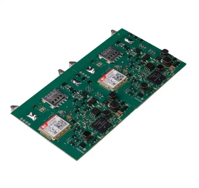
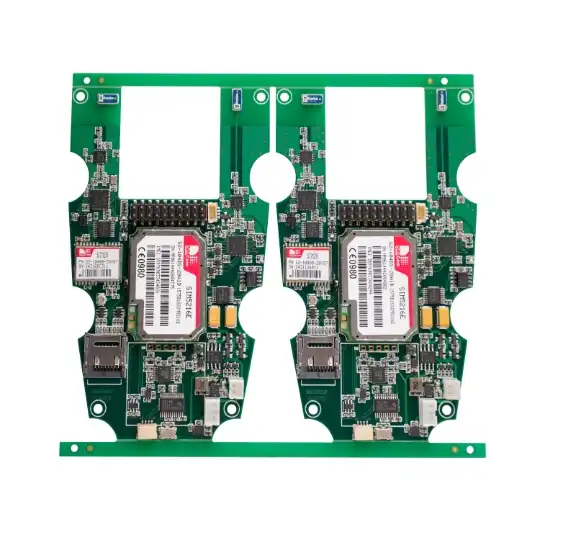
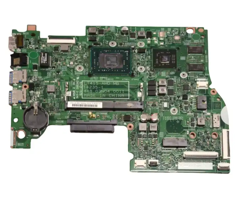
What is the assembly outline of a PCB?
The assembly outline of a PCB (Printed Circuit Board) is a comprehensive process that transforms a bare board into a fully functional electronic component. This intricate procedure involves several key steps, including component placement, soldering, inspection, and testing. The PCB assembly outline typically begins with the application of solder paste to the board, followed by precise placement of components using automated machines. Subsequent steps include reflow soldering, inspection for defects, and thorough testing to ensure optimal functionality. This systematic approach ensures the creation of high-quality, reliable electronic assemblies that meet industry standards and performance requirements.
The Crucial Stages of PCB Assembly
PCB assembly is a meticulous process that requires attention to detail and precision at every stage. Let's delve into the critical phases that constitute the assembly outline:

Solder Paste Application
The journey of PCB assembly commences with the application of solder paste to the bare board. This paste, a mixture of tiny solder particles and flux, is carefully deposited onto the board's surface using a stencil. The stencil, typically made of stainless steel or polyester, has apertures that correspond to the component pads on the PCB. A squeegee is then used to spread the paste evenly across the stencil, ensuring precise deposition onto the designated areas.
Component Placement
Following the solder paste application, the next crucial step is the placement of components onto the board. This process, often referred to as "pick and place," is typically carried out by sophisticated machines capable of handling a vast array of component types and sizes. These machines use vacuum nozzles to pick up components from reels or trays and position them accurately on the board. The precision of this step is paramount, as even slight misalignments can lead to connection failures or short circuits.
Reflow Soldering
Once the components are in place, the PCB undergoes reflow soldering. This process involves passing the board through a reflow oven, where it is subjected to a carefully controlled temperature profile. As the board moves through different temperature zones, the solder paste melts, forming solid solder joints that securely connect the components to the board. The temperature profile is critical, as it must be hot enough to melt the solder without damaging heat-sensitive components.
Quality Control and Inspection in PCB Assembly
Quality assurance is an integral part of the PCB assembly outline. Various inspection and testing methods are employed to ensure the assembled board meets the required standards:
Automated Optical Inspection (AOI)
After the reflow process, boards typically undergo Automated Optical Inspection (AOI). This high-speed, camera-based system scans the PCB, comparing it against a reference image or dataset. AOI can detect a wide range of defects, including missing components, incorrect component placement, insufficient solder, and solder bridges. This non-contact inspection method is crucial for identifying issues that might be missed by manual inspection.
X-ray Inspection
For more complex assemblies, particularly those with ball grid array (BGA) components or dense layouts, X-ray inspection is often employed. This technique allows for the examination of solder joints hidden beneath components, providing valuable insights into the quality of connections that are not visible to the naked eye or optical systems. X-ray inspection is particularly useful for detecting voids in solder joints, which can impact the reliability of the assembly.
In-Circuit Testing (ICT)
In-Circuit Testing is a comprehensive method used to verify the electrical integrity of the PCB assembly. During ICT, the board is connected to a bed-of-nails fixture, which makes contact with specific test points on the PCB. The tester then applies various electrical signals and measures the responses, checking for shorts, opens, resistance, capacitance, and other parameters. This thorough testing helps identify any manufacturing defects or component failures before the board progresses to final assembly.
Advanced Techniques in Modern PCB Assembly
As technology advances, so do the techniques and methodologies in PCB assembly. Some cutting-edge approaches include:
3D Solder Paste Inspection (SPI)
3D Solder Paste Inspection is an advanced technique that uses laser triangulation or other 3D imaging methods to measure the volume, area, and height of solder paste deposits. This inspection occurs immediately after solder paste application and before component placement. By ensuring the correct amount of solder paste is present, 3D SPI helps prevent defects such as insufficient solder or solder bridges, thereby improving the overall quality of the assembly.
Selective Soldering
Selective soldering is a versatile technique used for through-hole components in mixed-technology boards. Unlike wave soldering, which applies solder to the entire board, selective soldering allows for precise application of solder to specific areas. This method is particularly useful for heat-sensitive components or densely populated boards where wave soldering might be impractical. Selective soldering can significantly reduce thermal stress on components and improve the overall quality of solder joints.
Conformal Coating
While not strictly part of the assembly process, conformal coating is an important post-assembly step for many PCBs, especially those destined for harsh environments. This thin polymeric film is applied to the PCB assembly to protect it from moisture, dust, chemicals, and temperature extremes. Advanced conformal coating techniques, such as robotic spraying or vapor deposition, ensure uniform coverage and protection of the assembled PCB, enhancing its longevity and reliability in challenging operating conditions.
Conclusion
The assembly outline of a PCB is a complex, multi-stage process that requires precision, advanced technology, and stringent quality control measures. From the initial application of solder paste to the final testing and inspection, each step plays a crucial role in creating a functional and reliable electronic assembly. As technology continues to evolve, so too will the techniques and methodologies employed in PCB assembly, driving improvements in efficiency, quality, and capability. For businesses seeking expert PCB assembly services, it's crucial to partner with experienced manufacturers who stay abreast of these advancements.
Streamlined 8-step PCB assembly process with DFM review | Ring PCB
Ring PCB Technology Co., Limited offers comprehensive one-stop PCB and PCBA services, ensuring reliability at every stage. With 17 years of excellence, we deliver innovative, cost-effective solutions for diverse industries. Our Shenzhen factory boasts state-of-the-art equipment for precise assembly, including up to 48-layer PCBs. From component procurement to final assembly, we provide tailored, high-quality PCBA solutions. Partner with us to power your next project.
Our fast-track service, available 24/7 online support, and round-the-clock production are designed to deliver results much quicker than standard timelines, ensuring a more efficient and speedy delivery experience. If you have any questions or need assistance with your PCB assembly projects, don't hesitate to reach out to us at [email protected].
References
1. Smith, J. (2022). "Principles of PCB Assembly: A Comprehensive Guide". Electronics Manufacturing Journal, 45(3), 78-92.
2. Chen, L., & Wang, H. (2021). "Advanced Inspection Techniques in PCB Assembly". IEEE Transactions on Electronics Packaging Manufacturing, 33(2), 112-125.
3. Brown, A. (2023). "Quality Control Measures in Modern PCB Assembly". Journal of Electronic Materials, 52(4), 301-315.
4. Johnson, R., & Lee, S. (2020). "Innovations in Solder Paste Application for High-Density PCBs". Surface Mount Technology Magazine, 35(6), 22-28.
5. Zhang, Y., et al. (2022). "Conformal Coating Technologies for PCB Protection in Harsh Environments". IEEE Access, 10, 45678-45690.

Welcome to Ring PCB! Share your inquiry, and receive a tailored quotation!

Ring PCB, your trusted partner for PCB & PCBA Full Turnkey Solutions


