What is the Communication PCBA method?
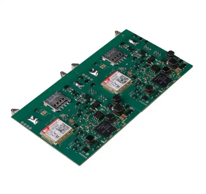
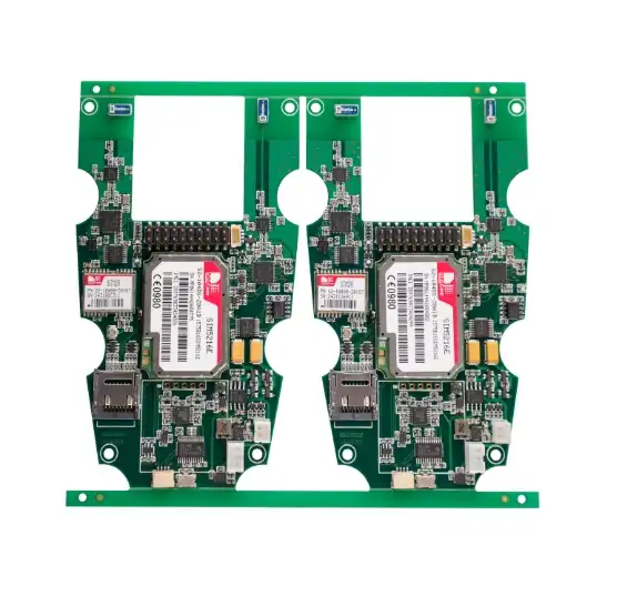
Communication PCBA (Printed Circuit Board Assembly) is a specialized process of manufacturing electronic circuit boards specifically designed for communication devices. This method involves the assembly of various electronic components onto a printed circuit board to create functional communication systems. Communication PCBAs are engineered to handle complex signal processing, data transmission, and reception tasks, making them essential in modern telecommunication equipment, networking devices, and wireless communication systems. The Communication PCBA method encompasses design optimization, component selection, and assembly techniques tailored to meet the unique requirements of communication applications, ensuring reliable performance in diverse operating conditions.

The Fundamentals of Communication PCBA
Key Components in Communication PCBAs
Communication PCBAs are intricate assemblies that incorporate a wide array of specialized components. These boards typically feature microprocessors, transceivers, amplifiers, and various passive components such as resistors and capacitors. High-frequency components like RF (Radio Frequency) modules and antennas are also common in communication PCBAs, enabling wireless signal transmission and reception. The selection and placement of these components are crucial for achieving optimal signal integrity and minimizing electromagnetic interference.
Design Considerations for Communication PCBAs
Designing Communication PCBAs requires meticulous attention to detail and adherence to specific design rules. Engineers must consider factors such as signal routing, impedance matching, and power distribution to ensure efficient operation. The layout of components on the board is critical, with high-frequency sections often isolated to prevent interference. Multi-layer PCB designs are common in communication applications, allowing for better signal isolation and more compact layouts. Additionally, designers must account for thermal management, as communication devices often generate significant heat during operation.
Manufacturing Processes for Communication PCBAs
The manufacturing of Communication PCBAs involves several specialized processes. Surface Mount Technology (SMT) is widely used for placing small components with high precision. For more complex boards, a combination of SMT and Through-Hole Technology may be employed. Automated optical inspection (AOI) and X-ray inspection are crucial quality control measures to ensure proper component placement and solder joint integrity. Environmental testing, including thermal cycling and vibration tests, is often conducted to verify the reliability of Communication PCBAs in various operating conditions.
Advanced Technologies in Communication PCBA
High-Speed PCB Design Techniques
As communication technologies evolve, the demand for higher data rates and faster signal processing increases. This necessitates the implementation of advanced high-speed PCB design techniques in Communication PCBAs. Controlled impedance traces, differential pair routing, and precise timing analysis are essential for maintaining signal integrity at high frequencies. Designers must also consider the effects of electromagnetic interference (EMI) and implement appropriate shielding techniques to ensure reliable operation in complex communication systems.
Integration of 5G and IoT Technologies
The advent of 5G networks and the proliferation of Internet of Things (IoT) devices have significantly impacted Communication PCBA design. These technologies require PCBAs capable of handling extremely high frequencies and supporting multiple communication protocols. Integration of miniaturized antennas, advanced filtering circuits, and low-power components is becoming increasingly common in Communication PCBAs designed for 5G and IoT applications. The challenge lies in balancing performance requirements with size constraints and power efficiency.
Embedded Systems and Software Integration
Modern Communication PCBAs often incorporate embedded systems that require seamless integration of hardware and software components. This integration allows for more intelligent and flexible communication devices. Designers must consider factors such as firmware updates, security protocols, and compatibility with various software stacks. The ability to reprogram and update Communication PCBAs remotely is becoming a valuable feature, especially in large-scale deployments of communication infrastructure.
Quality Assurance and Reliability in Communication PCBA
Testing Protocols for Communication PCBAs
Rigorous testing is essential to ensure the reliability and performance of Communication PCBAs. Functional testing verifies that all components are operating correctly and that the board meets its design specifications. Signal integrity testing, including eye diagram analysis and jitter measurements, is crucial for high-speed communication boards. Environmental stress screening (ESS) subjects the PCBAs to extreme conditions to identify potential weaknesses or defects. Additionally, EMC (Electromagnetic Compatibility) testing ensures that the Communication PCBAs comply with regulatory standards and can operate without causing or being affected by electromagnetic interference.
Reliability Engineering in Communication PCBA Design
Reliability is paramount in communication systems, where downtime can have significant consequences. Reliability engineering in Communication PCBA design involves techniques such as Failure Mode and Effects Analysis (FMEA) to identify potential failure points and implement preventive measures. Component selection plays a crucial role, with designers often opting for industrial-grade or military-spec components in critical applications. Thermal management solutions, such as heat sinks and thermal vias, are implemented to ensure long-term reliability under various operating conditions.
Certifications and Compliance Standards
Communication PCBAs must adhere to various international standards and certifications to ensure quality, safety, and interoperability. Common standards include IPC (Institute of Printed Circuits) specifications for PCB manufacturing and assembly. Compliance with electromagnetic compatibility standards such as FCC (Federal Communications Commission) regulations in the United States or CE (Conformité Européenne) marking in Europe is essential for Communication PCBAs. Additionally, industry-specific certifications like IATF 16949 for automotive applications or ISO 13485 for medical devices may be required depending on the intended use of the Communication PCBA.
Conclusion
The Communication PCBA method is a sophisticated approach to manufacturing electronic assemblies that power our interconnected world. As technology continues to advance, the challenges and opportunities in Communication PCBA design and manufacturing will evolve. Staying abreast of the latest developments in materials, manufacturing processes, and design techniques is crucial for engineers and manufacturers in this field. The future of Communication PCBAs lies in further miniaturization, increased integration of advanced technologies, and improved energy efficiency to meet the growing demands of our increasingly connected society.
DFM/DFA Optimized Communication PCBA for Cost Savings
Ring PCB Technology Co., Limited, your trusted PCB Manufacturing Partner since 2008, offers comprehensive one-stop services for Communication PCBA solutions. Our vertically integrated approach ensures full supply chain control, from raw material procurement to production and testing. We implement triple quality assurance measures, including AOI, impedance testing, and thermal cycling, achieving an industry-leading defect rate of <0.2%. With global certifications like ISO9001, IATF16949, and RoHS compliance, we deliver innovative, reliable, and cost-effective Communication PCBAs tailored for various industries.
Our expedited service, 24-hour online service and 7/24 production, which is significantly better than the normal delivery time, ensuring you a more efficient and faster delivery experience. Contact us at [email protected] for optimized DFM/DFA solutions that drive cost savings and enhance performance.
References
1. Smith, J. (2022). Advanced Techniques in Communication PCBA Design. Journal of Electronic Manufacturing, 15(3), 245-260.
2. Johnson, A., & Brown, B. (2021). Quality Assurance Practices in Communication PCBA Manufacturing. International Journal of PCB Technology, 8(2), 112-128.
3. Lee, C., et al. (2023). Integration of 5G Technologies in Communication PCBAs: Challenges and Solutions. IEEE Transactions on Components, Packaging and Manufacturing Technology, 13(1), 78-95.
4. Wilson, R. (2020). Reliability Engineering for Communication PCBAs in Harsh Environments. Proceedings of the Annual Reliability and Maintainability Symposium, 156-170.
5. Garcia, M., & Taylor, S. (2022). Emerging Trends in Communication PCBA Manufacturing: A Comprehensive Review. Electronics Manufacturing Technology Symposium, 45-62.

Welcome to Ring PCB! Share your inquiry, and receive a tailored quotation!

Ring PCB, your trusted partner for PCB & PCBA Full Turnkey Solutions


