Understanding PCB Inspection Methodologies
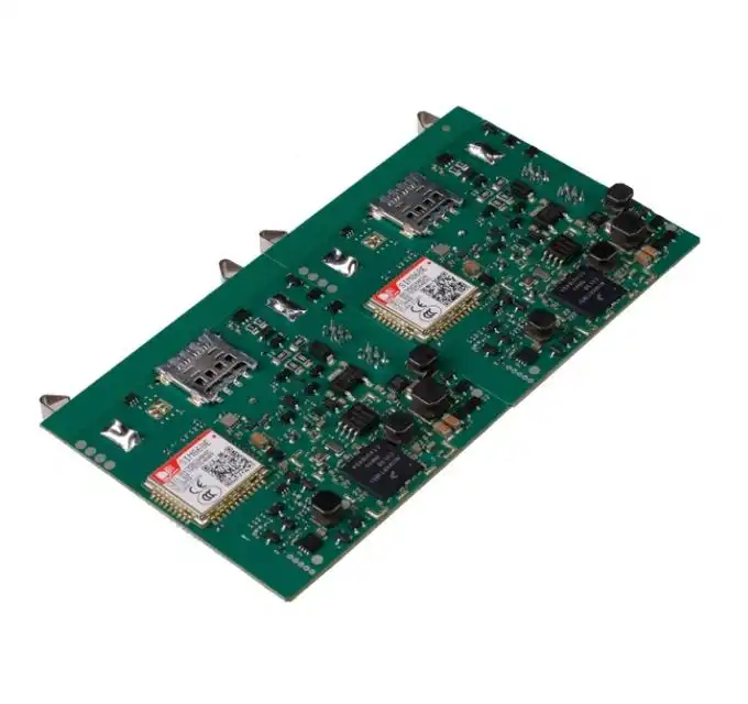
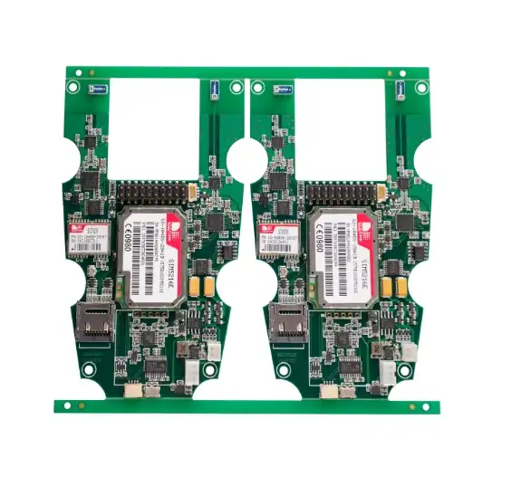
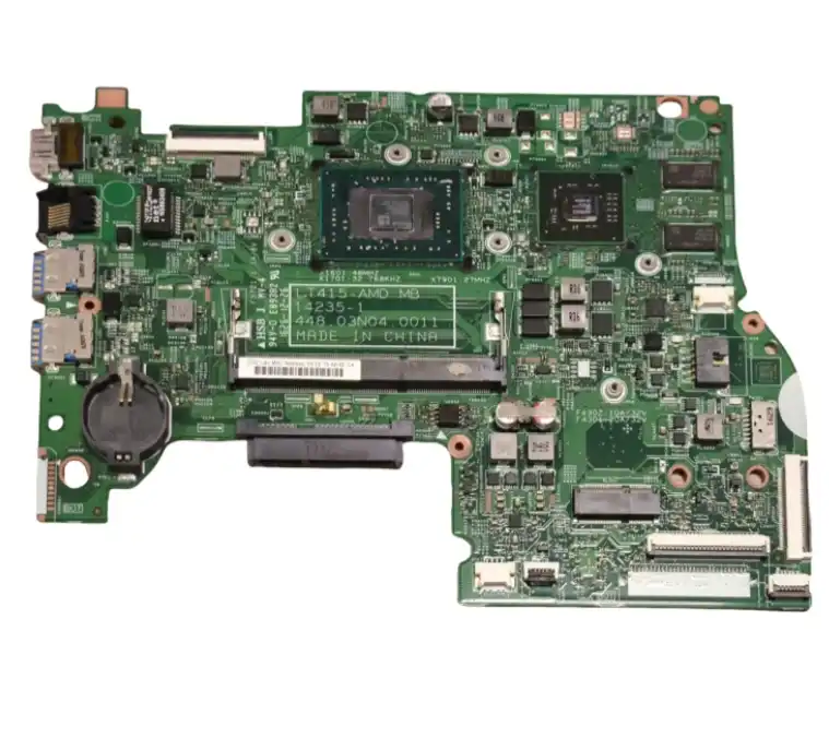
PCB inspection is a critical process in ensuring the quality and reliability of printed circuit boards. It encompasses various techniques and technologies aimed at identifying defects, verifying assembly accuracy, and validating overall board functionality. As PCB designs become increasingly complex, with high-density interconnects (HDI) and multilayer structures, the importance of thorough inspection grows exponentially.
Visual Inspection Techniques
Visual inspection forms the foundation of PCB quality control. It includes both manual and automated optical inspection (AOI) methods. Manual inspection relies on skilled technicians using magnification tools to examine boards for visible defects. AOI systems employ high-resolution cameras and advanced image processing algorithms to detect issues such as missing components, solder defects, and incorrect component placement. These systems are particularly effective for surface mount technology (SMT) assemblies, where component sizes are often too small for reliable manual inspection.
X-ray Inspection for Hidden Defects
X-ray inspection is invaluable for examining internal layers of multilayer PCBs and detecting hidden defects in ball grid array (BGA) and other complex package types. This non-destructive testing method allows inspectors to visualize solder joints, vias, and internal connections that are not visible to the naked eye or traditional optical inspection methods. X-ray systems are particularly crucial for high-reliability applications in automotive, aerospace, and medical industries, where internal defects could lead to catastrophic failures.

Electrical Testing Methodologies
Electrical testing is essential for verifying the functionality and performance of assembled PCBs. This category includes in-circuit testing (ICT), which checks individual components and connections, and functional testing, which evaluates the board's overall performance under simulated operating conditions. For high-frequency or high-speed designs, specialized testing such as signal integrity analysis and impedance control verification may be necessary to ensure optimal performance.
Advantages and Limitations of 100% PCB Inspection
Implementing 100% PCB inspection offers several significant benefits but also comes with certain limitations that must be carefully considered in the context of production requirements and quality goals.
Benefits of Comprehensive Inspection
The primary advantage of 100% inspection is the potential to catch all defects before products reach the end-user. This approach is particularly beneficial for high-reliability applications, such as automotive-grade PCBs or industrial-grade assemblies, where even a single failure could have severe consequences. Full inspection also provides valuable data for continuous process improvement, allowing manufacturers to identify and address recurring issues in their assembly processes.
For complex multilayer PCBs or those with microvia structures, 100% inspection helps ensure that intricate internal connections and high-density areas are thoroughly examined. This level of scrutiny is often necessary for new product introductions or when implementing challenging design features, such as flexible or rigid-flex PCBs, where the risk of defects may be higher.
Challenges and Considerations
While comprehensive, 100% inspection can be time-consuming and resource-intensive, potentially impacting production throughput. The cost of equipment, such as advanced X-ray systems or automated optical inspection machines, can be substantial, especially for smaller production runs. Additionally, the vast amount of data generated by full inspection requires sophisticated analysis tools and skilled personnel to interpret results effectively.
There's also the risk of false positives, where benign anomalies are flagged as defects, leading to unnecessary rework or scrapping of good boards. Balancing sensitivity and specificity in inspection criteria is crucial to avoid these issues while maintaining high quality standards.
Sample Testing: Strategies and Best Practices
Sample testing offers a more targeted approach to PCB inspection, focusing on statistical methods to infer overall quality from a subset of the production run. This method can be highly effective when properly implemented, especially for high-volume production where 100% inspection may not be feasible or cost-effective.
Designing Effective Sampling Plans
The key to successful sample testing lies in developing robust sampling plans that accurately represent the entire production batch. Factors to consider include production volume, historical defect rates, and the criticality of the application. Acceptance Quality Limit (AQL) sampling is a common approach, where the sample size and acceptance criteria are determined based on the desired quality level and the risk tolerance for accepting defective units.
For PCB assemblies with varying complexity levels, stratified sampling techniques can be employed. This involves dividing the production batch into subgroups based on factors like board complexity or assembly process, and then sampling from each group to ensure comprehensive coverage.
Integrating Sample Testing with Process Control
Sample testing should not be viewed in isolation but as part of a broader quality control strategy. Integrating sample inspection results with statistical process control (SPC) methods can provide insights into process trends and early warning signs of quality issues. This proactive approach allows manufacturers to adjust their processes before significant problems arise, maintaining high quality standards while optimizing inspection resources.
For PCB manufacturers offering one-stop PCBA services, sample testing can be strategically applied at different stages of the production process. For instance, more intensive sampling might be used during initial setup and pilot runs, with reduced sampling frequency once processes are stabilized and proven reliable.
Conclusion
The choice between 100% PCB inspection and sample testing is not a one-size-fits-all decision. It requires careful consideration of product requirements, production volumes, and quality objectives. For high-reliability applications, complex designs, or new product introductions, 100% inspection provides the highest level of assurance. However, for established, high-volume production with consistent quality, well-designed sample testing strategies can offer an effective balance between quality assurance and operational efficiency.
Ultimately, many PCB manufacturers and PCBA suppliers opt for a hybrid approach, combining elements of both methods. This might involve 100% inspection for critical features or high-risk areas, complemented by sample testing for more stable aspects of production. The key is to develop a flexible, data-driven inspection strategy that evolves with changing product requirements and production capabilities.
By leveraging advanced inspection technologies such as AOI, X-ray, and electrical testing, alongside robust sampling methodologies, PCB assembly manufacturers can ensure high-quality outputs while optimizing their production processes. This comprehensive approach to quality control is essential for meeting the demanding requirements of industries such as automotive, aerospace, and medical electronics, where reliability and performance are paramount.
FAQ
What are the main differences between 100% PCB inspection and sample testing?
100% inspection examines every board produced, offering maximum defect detection but at higher cost and time investment. Sample testing inspects a representative subset, balancing efficiency with acceptable quality levels.
How does PCB complexity affect the choice of inspection method?
More complex PCBs, such as multilayer or HDI designs, often benefit from 100% inspection due to their intricate structures and higher defect risks. Simpler designs may be suitable for sample testing.
Can automated systems like AOI replace manual inspection entirely?
While AOI significantly enhances inspection capabilities, a combination of automated and manual methods often provides the most comprehensive quality assurance, especially for complex or critical applications.
Expert PCB Inspection and Assembly Services | Ring PCB
At Ring PCB, we offer comprehensive PCB inspection and assembly services tailored to your specific needs. Our state-of-the-art facility employs advanced AOI, X-ray, and functional testing technologies to ensure the highest quality standards for your PCB projects. Whether you require 100% inspection for critical applications or efficient sample testing for high-volume production, our experienced team delivers reliable, cost-effective solutions. Contact us at [email protected] to learn how our expertise in multilayer PCB manufacturing, HDI PCB assembly, and turnkey PCBA services can elevate your product quality and reliability.


