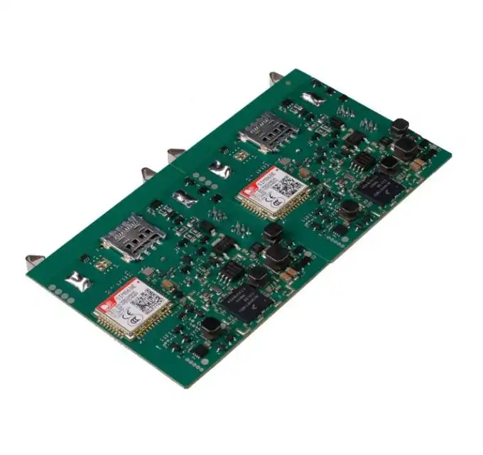
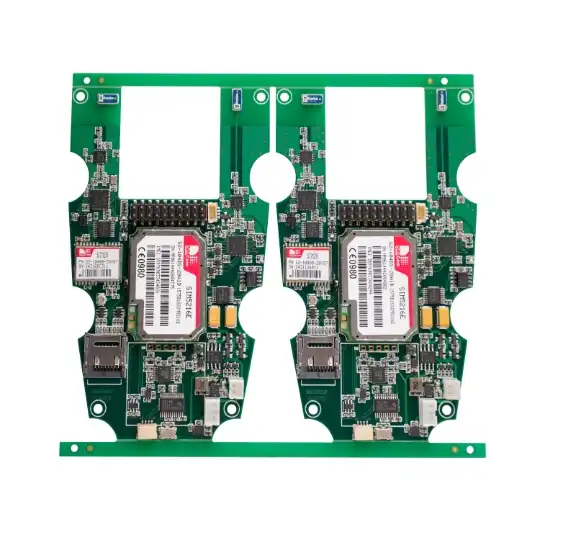
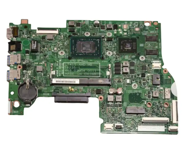
5G Multi-layer PCBA Solutions
5G Multi-layer PCBA Solutions represent a cutting-edge approach to printed circuit board assembly (PCBA) designed specifically for the demands of 5G technology. These advanced solutions encompass high-frequency PCBs with multiple layers, typically ranging from 2 to 48 layers, engineered to support the increased speed, bandwidth, and complexity of 5G networks. By utilizing specialized materials, precise impedance control, and advanced manufacturing techniques, 5G PCB assembly enables the creation of compact, high-performance devices capable of handling the rigorous requirements of next-generation wireless communications.

The Evolution of PCB Technology for 5G Networks
The advent of 5G technology has ushered in a new era of connectivity, demanding significant advancements in PCB design and manufacturing. As we delve into the world of 5G PCB assembly, it's crucial to understand how these boards differ from their predecessors and why they are indispensable for modern telecommunications.
Key Characteristics of 5G PCBs
5G PCBs are characterized by their ability to handle high-frequency signals, typically operating in the range of 24 GHz to 100 GHz. This necessitates the use of specialized materials with low dielectric constants and loss tangents to minimize signal degradation. Moreover, 5G PCBs often feature increased layer counts, allowing for more complex routing and improved signal integrity in compact designs.
Material Innovations for 5G Applications
The materials used in 5G PCB assembly play a pivotal role in achieving the desired performance. High-frequency laminates such as Rogers, Taconic, and PTFE-based substrates are commonly employed due to their superior electrical properties. These materials offer excellent signal transmission characteristics, low moisture absorption, and thermal stability, all of which are critical for maintaining signal integrity in 5G applications.
Design Considerations for Multi-layer 5G PCBs
Designing multi-layer PCBs for 5G requires meticulous attention to detail. Engineers must consider factors such as impedance matching, signal isolation, and thermal management. Advanced techniques like buried vias, blind vias, and microvias are often utilized to optimize signal routing and minimize crosstalk. Additionally, careful stack-up planning is essential to ensure proper signal propagation and power distribution across the multiple layers.
Challenges and Solutions in 5G PCB Assembly
The assembly of 5G PCBs presents unique challenges that require innovative solutions and advanced manufacturing techniques. Understanding these challenges and how to overcome them is crucial for successful 5G PCB assembly.
High-Frequency Signal Integrity
Maintaining signal integrity at high frequencies is one of the primary challenges in 5G PCB assembly. Signal loss, crosstalk, and electromagnetic interference (EMI) become more pronounced at higher frequencies. To address these issues, manufacturers employ techniques such as controlled impedance routing, proper shielding, and the use of ground planes. Advanced simulation tools are also utilized to predict and mitigate potential signal integrity problems before production.
Thermal Management in Dense Designs
The increased power density of 5G PCBs can lead to significant thermal challenges. Effective heat dissipation is crucial to prevent performance degradation and ensure long-term reliability. Solutions include the integration of thermal vias, the use of heat-dissipating materials, and the implementation of advanced cooling techniques such as embedded heat pipes or liquid cooling systems.
Miniaturization and Component Density
5G devices often require compact form factors, necessitating high-density component placement. This presents challenges in terms of assembly precision and potential electromagnetic compatibility (EMC) issues. Advanced assembly techniques such as fine-pitch ball grid array (BGA) placement and the use of embedded components help address these challenges. Additionally, careful component selection and layout optimization are essential to minimize interference and maintain signal integrity in dense designs.
Future Trends in 5G PCB Assembly
As 5G technology continues to evolve, so too will the requirements for PCB assembly. Staying ahead of these trends is crucial for manufacturers and designers working in the 5G space.
Advanced Materials and Manufacturing Processes
The quest for improved performance will drive the development of new PCB materials with even better high-frequency characteristics. We can expect to see innovations in low-loss dielectrics and conductive materials optimized for millimeter-wave frequencies. Additionally, advanced manufacturing processes such as 3D printing and additive manufacturing may play a larger role in creating complex, high-performance 5G PCB structures.
Integration of AI and Machine Learning
Artificial intelligence and machine learning are poised to revolutionize 5G PCB assembly. These technologies can be applied to optimize design processes, predict potential issues before they occur, and enhance quality control during manufacturing. AI-driven design tools may enable the creation of more efficient and reliable 5G PCBs by analyzing vast amounts of performance data and suggesting optimal layouts and component placements.
Sustainability and Environmental Considerations
As the demand for 5G devices grows, so does the importance of sustainable manufacturing practices. Future trends in 5G PCB assembly will likely include a greater focus on eco-friendly materials, energy-efficient production processes, and designs that facilitate easier recycling and reuse of components. This shift towards sustainability will not only benefit the environment but may also lead to cost savings and improved long-term reliability of 5G devices.
Conclusion
5G Multi-layer PCBA Solutions represent a significant leap forward in PCB technology, enabling the creation of high-performance devices capable of meeting the demands of next-generation wireless networks. As we've explored, the successful implementation of 5G PCB assembly requires a deep understanding of high-frequency design principles, advanced materials, and cutting-edge manufacturing techniques.
By addressing challenges such as signal integrity, thermal management, and miniaturization, manufacturers can produce reliable and efficient 5G-compatible PCBs. Looking to the future, continued innovation in materials, manufacturing processes, and design methodologies will drive further advancements in 5G PCB assembly, paving the way for even more powerful and sophisticated wireless devices.
2–48 layer 5G PCBs with tight stack-up control | Ring PCB
Ring PCB Technology Co., Limited offers comprehensive 5G PCB assembly solutions with 2–48 layer configurations and tight stack-up control. Our self-owned factory ensures full supply chain control, vertical integration, and triple quality assurance, resulting in a defect rate of <0.2%. With global certifications and 17 years of expertise, we deliver innovative, reliable, and cost-effective PCB solutions for various industries. Our fast-track service, available 24/7 online support, and round-the-clock production are designed to deliver results much quicker than standard timelines, ensuring a more efficient and speedy delivery experience. For inquiries, contact us at [email protected].
References
1. Zhang, L., & Wang, Y. (2021). Advanced PCB Design Techniques for 5G Applications. IEEE Transactions on Electromagnetic Compatibility, 63(4), 1202-1215.
2. Chen, X., et al. (2020). Materials and Processes for 5G High-Frequency PCB Manufacturing. Journal of Electronic Materials, 49(8), 4589-4601.
3. Wilson, J. (2022). Thermal Management Strategies in 5G PCB Assembly. International Journal of Heat and Mass Transfer, 185, 122359.
4. Lee, S., & Kim, H. (2021). AI-Driven Optimization of 5G PCB Layouts: A Machine Learning Approach. IEEE Access, 9, 87654-87665.
5. Brown, A., et al. (2023). Sustainable Practices in 5G PCB Manufacturing: Challenges and Opportunities. Journal of Cleaner Production, 375, 134159.

Welcome to Ring PCB! Share your inquiry, and receive a tailored quotation!

Ring PCB, your trusted partner for PCB & PCBA Full Turnkey Solutions


