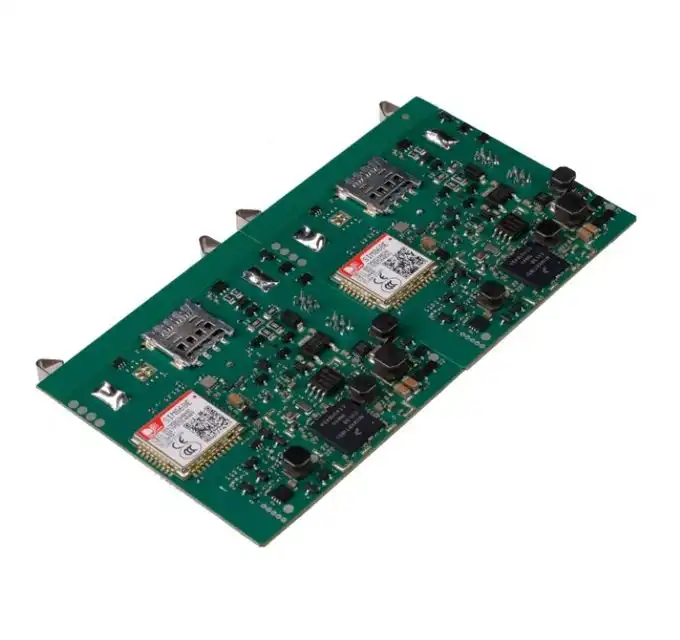
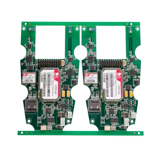
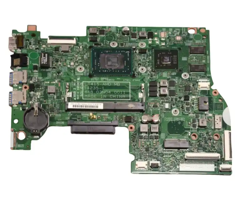
The highest level of electronic engineering is represented by complex multilayer PCB manufacture and assembly, which produces intricate circuit boards with eight or more layers that power the most cutting-edge electronic products available today. To provide small, high-performance solutions necessary for telecommunications, automotive, medical, and aerospace applications, multilayer PCB assembly entails complex procedures that integrate numerous conductive layers with dielectric material. These cutting-edge boards are essential for the creation of contemporary electronic products because they provide better signal integrity, better thermal management, and a higher circuit density than conventional single- or double-layer alternatives.
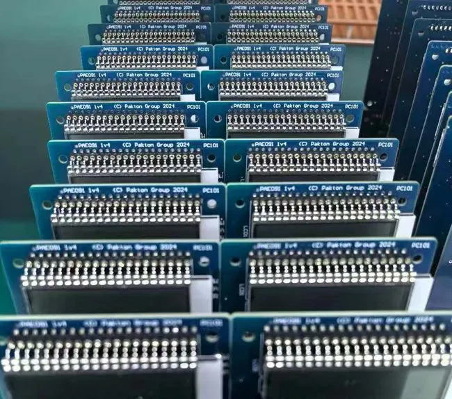
Understanding Complex Multilayer PCB Assembly
High-performance electronic solutions in cutting-edge industries like telecom, automotive, aerospace, and medicine are supported by complex multilayer PCB assemblies, which consist of eight or more layers. Compared to more straightforward options, these advanced boards allow for more circuit density, enhanced signal integrity, and better thermal management. B2B procurement specialists still need to comprehend the intricate production processes, such as laminating, drilling, plating, and soldering, in order to properly evaluate quality and dependability. Multilayer PCBs are essential in demanding applications that require durability and compactness because these procedures combine numerous material layers and precision assembly techniques to fulfill the high demands of current electronics.
What Is Multilayer PCB Assembly?
Printed circuit boards with three or more conducting layers separated by insulating materials are referred to as multilayer PCB assembly. Modern electronics have undergone a revolution because to this cutting-edge technology, which makes it possible for smaller designs with more functionality. Several copper layers are stacked using prepreg materials throughout the assembly process, and they are bonded together using pressure lamination and regulated temperature.
Multilayer PCBs have vital uses in a variety of businesses in today's B2B environment. These boards are necessary for 5G infrastructure and fast data transfer in telecommunications equipment. Multilayer designs are used in automotive electronics for sophisticated driver assistance systems, electric vehicle power management, and engine control units. These assemblies are used in imaging equipment, patient monitoring systems, and implanted devices that need dependable yet small electronics.
The Multilayer PCB Assembly Process Explained
Careful material selection and stack-up planning are the first steps in the production process. The layer layout is created by engineers to maximize temperature management, power distribution, and signal routing. All layers are combined during the lamination step, which usually reaches a temperature of 375°F and a pressure of 400 PSI.
The quality of the finished output is shaped by critical methods. Lamination preserves dimensional stability while guaranteeing appropriate layer bonding. Vias for interlayer connections are made via precision drilling, which demands tolerances of less than 0.001 inches. Surface mount technology (SMT) and through-hole component assembly come after copper plating, which creates electrical contact between layers. Strict quality control is required at every stage to avoid flaws that might jeopardize the assembly as a whole.
Advantages of Using Complex (8+ Layers) Multilayer PCBs
Compared to simpler options, complex multilayer PCBs have many benefits. For portable electronics and applications with limited space, designers may fit more functionality into smaller form factors by increasing circuit density. The many ground and power planes minimize signal crosstalk and provide superior electromagnetic interference (EMI) shielding in Multilayer PCB assembly.
Reduced parasitic effects and regulated impedance characteristics result in improved electrical performance. Appropriate ground plane arrangement and specialized signal layers enhance signal integrity. Increased copper content and the ability to disperse heat over many layers are advantageous for thermal management. More structural layers improve mechanical stability, which lowers component stress and board bending while in use.
Multilayer PCB Design Considerations for Complex Boards
Stack-up arrangement requires careful planning to balance cost, manufacturing feasibility, and electrical performance. For high-speed communications, engineers must manage dielectric constants, layer thickness, and impedance within a tolerance of ±7%. Performance and cost are affected by the choice of material; FR-4 is used for ordinary applications, whereas Rogers and other specialty materials are used for high-frequency needs.
Manufacturing yield and signal integrity are greatly impacted by design approach. While buried vias only connect internal layers, blind vias connect exterior layers to interior levels without piercing the whole board. Microvias enhance fine-pitch components and compact layouts by enabling greater density routing in HDI (High Density Interconnect) systems.
Comparing Multilayer PCB Assembly with Other PCB Types
Knowing the differences between multilayer, single-layer, double-layer, rigid, and flexible printed circuit boards (PCBs) is essential when choosing PCBs for intricate electrical goods. Multilayer PCBs are the favored option for complicated applications because they provide better circuit density and performance at a greater cost and complexity. various design requirements, such bending or small form factors, are addressed by rigid and flexible multilayer PCBs, necessitating various materials and manufacturing processes. In the B2B manufacturing sector, optimal project results and maximized product dependability are ensured by identifying frequent assembly obstacles, such as layer alignment and signal integrity concerns, and being aware of appropriate mitigation techniques.
Multilayer vs Single Layer and Double Layer PCB Assembly
Performance and cost are greatly impacted by the complexity difference between multilayer and simpler PCB variants. Single-layer boards are appropriate for simple applications with low component densities and straightforward routing specifications. Compared to single-layer alternatives, double-layer PCBs provide more routing flexibility and can handle intermediate complexity.
When projects need for intricate routing, high component density, or exceptional electrical performance, multilayer assemblies perform very well. Multilayer boards may be three to ten times more expensive, but the investment pays out in smaller products, better performance, and increased dependability. The multilayer technique is usually justified by applications that need high-speed digital signals, analog circuits with stringent noise requirements, or small form factors.
Rigid vs Flexible Multilayer PCB Assembly
Traditional applications where cost reduction and mechanical stability are crucial are dominated by rigid multilayer PCBs. These boards are appropriate for the majority of electronic goods since they are made using standard FR-4 materials and traditional production techniques. For large-scale manufacturing, expenses are kept reasonable while manufacturing tolerances are maintained in Multilayer PCB assembly.
Specialized applications that call for three-dimensional packing or bending capabilities are served by flexible multilayer systems. Flexible designs are used by sectors including wearable electronics, medical devices, and aircraft to save space and ensure mechanical compliance. Although polyimide substrates and specialty adhesives are more expensive, they allow for novel form factors that rigid boards cannot.
Common Challenges in Complex Multilayer PCB Assembly and How to Overcome Them
In multilayer assembly, layer alignment is the main obstacle since misalignment may result in electrical failures and decreased yield. Precision tooling and optical registration technologies are used in modern production to maintain alignment within ±0.001 inches. Controlled pressure and temperature profiles suited to particular material combinations are necessary to prevent lamination faults like delamination or void formation.
The number of layers and frequency requirements increase the number of signal integrity problems. Ground plane management, via optimization, and appropriate impedance control are effective methods. While sophisticated simulation techniques forecast performance prior to actual prototypes, design for manufacturability (DFM) studies identify possible issues early. By lowering failure rates, these mitigation techniques improve the general dependability of the product.
Best Practices and Techniques for High-Quality Multilayer PCB Assembly
Advanced manufacturing procedures, such as precise stack-up lamination, accurate drilling, and stringent inspection techniques like Automated Optical Inspection (AOI) and X-ray testing, are necessary to produce high-quality 8+ layer multilayer PCBs. Defects may be found early, waste can be decreased, and yield rates can be increased by putting in place comprehensive quality control and failure analysis procedures. To choose the best assembly choice, it is necessary to comprehend material influences, production scale, and performance aims in order to balance cost and quality. For B2B procurement specialists looking for trustworthy suppliers that can provide multilayer PCB assemblies that satisfy strict industry requirements, these best practices are still crucial.
Proven Techniques for Manufacturing 8+ Layer PCBs
Consistent layer bonding and dimensional stability are guaranteed by sophisticated stack-up lamination processes. In order to eliminate air bubbles and achieve consistent thickness across the panel, modern facilities use vacuum lamination presses with precise temperature and pressure control. When compared to traditional photolithography, LDI (Laser Direct Imaging) exposure methods provide better pattern resolution and registration accuracy.
As the number of layers and via density grow, drilling accuracy becomes crucial. Advanced spindle control in mechanical drilling systems maintains hole quality and location precision within ±0.0005 inches. While X-ray examination shows internal flaws that surface inspection techniques are unable to detect, automated optical inspection (AOI) devices confirm the quality of drill holes. In high-layer-count assemblies, these technologies work together to provide constant quality.
Quality Control and Failure Analysis in Multilayer PCB Assembly
Decisions about production and customer satisfaction are guided by thorough quality measures. Dimensional precision, electrical continuity, impedance control, and visual defect rates are important factors. Depending on the complexity of the assembly and the needs of the client, testing procedures include flying probe testing, in-circuit testing (ICT), and functional verification.
Protocols for failure analysis aid in identifying underlying issues and averting recurrence. Electrical shorts or openings, solder joint flaws, and incorrect component placement are common failure modes. Continuous improvement and yield optimization are made possible by statistical process control, which monitors important parameters throughout time. Stronger supplier connections, increased customer satisfaction, and waste reduction are all benefits of effective failure analysis.
Cost vs Quality: Evaluating Multilayer PCB Assembly Options
Factors affecting assembly costs include manufacturing volume, layer count, technology, and material choice. Although they are more expensive, high-performance materials such as low-loss dielectrics allow for better electrical performance. Density and cost are impacted by technological decisions; microvias increase functionality at a greater cost.
A thorough grasp of application requirements and design limitations is necessary to strike a balance between pricing and performance. Because of economies of scale and improved manufacturing techniques, volume production usually lowers per-unit costs. Higher initial expenditures may be justified by long-term reliability concerns for crucial applications where field failures have serious repercussions.
Procuring Complex Multilayer PCB Assembly Services: What B2B Clients Need to Know
Purchasing sophisticated multilayer PCB assembly services requires a thorough partner assessment to make sure capacity, expertise, and quality match project specifications. Production is streamlined and time-to-market is decreased by selecting suppliers that have the necessary certifications, a track record of success, and the capacity to provide turnkey solutions, which include sourcing, assembly, testing, and shipping. B2B customers are better equipped to manage their budgets and negotiate advantageous terms when they have a thorough understanding of lead times, minimum order quantities (MOQs), and pricing strategies. With this information, procurement teams may choose dependable, scalable partners for multilayer PCB assembly that facilitate both the prototype and mass production stages.
How to Choose a Reliable Multilayer PCB Assembly Partner?
Certifications, manufacturing expertise, and production capacity are among the fundamental selection factors. IPC-6012 Class 3 compliance guarantees adherence to industry requirements for complicated assemblies, whereas ISO9001 and IATF16949 certifications signify established quality management systems. RoHS compliance and UL accreditation show a dedication to environmental and safety standards.
Examining case studies, customer reviews, and quality measurements are all part of assessing a supplier's performance history. Reputable vendors provide references from related fields and applications, showcasing their expertise and competence. Long-term partnership viability is shown by stable finances and ongoing investments in training and equipment.
Understanding Turnkey Multilayer PCB Assembly Services
By combining many supply chain components under single-source management, turnkey solutions simplify procurement. Component procurement, inventory control, assembly, testing, and logistics coordination are all included in these all-inclusive services. Benefits of speed and integration enhance project coordination and save administrative costs.
Design for Manufacturability (DFM) review, component procurement and verification, assembly and testing, and final delivery with documentation are all included in full turnkey solutions. This integrated strategy speeds up time-to-market and simplifies coordination while maintaining quality standards all the way through the manufacturing process.
Multilayer PCB Assembly Lead Time, MOQ, and Pricing Insights
Standard structures usually have prototype lead times of 5–10 days, whereas sophisticated HDI or exotic material needs might result in lead times of 15-20 days. For ordinary multilayer assemblies, mass production scheduling typically takes two to four weeks, depending on volume, complexity, and material availability.
Depending on supplier capabilities and complexity, different minimum order quantities apply. For prototypes, simple multilayer boards may have MOQs as low as 5–10 pieces, while sophisticated assemblies may need 25–50 pieces. Breaks in bulk pricing usually happen at quantities of 100, 500, and 1000 pieces or more, and yearly volume agreements may result in considerable cost savings.
Company Overview and Our Expertise in Complex Multilayer PCB Manufacturing
Ring PCB has a track record of expertise in producing and assembling intricate multilayer PCBs, with a focus on 8+ layer solutions for international B2B customers. With cutting-edge facilities and cutting-edge technology, we provide customized engineering assistance for anything from prototype development to mass manufacturing. Our product line offers a wide range of materials and assembly techniques that are intended to provide the best possible electrical performance and high dependability in Multilayer PCB assembly. We provide a smooth procurement process that supports the business objectives of our global customers while upholding strict quality standards and innovation leadership, all while using flexible logistics and prompt customer care.
Our Commitment to Quality and Innovation in PCB Assembly
Ring PCB produces exceptional multilayer PCB assemblies by fusing decades of industry experience with state-of-the-art production capabilities. Our in-house facility is equipped with cutting-edge machinery like as vacuum lamination presses, flying probe testers, and LDI laser exposure systems, which guarantee precise manufacture that complies with IPC-6012 Class 3 requirements.
48-layer boards with blind/buried vias, 3/3mil trace/spacing tolerances, and ±7% impedance control are examples of advanced manufacturing capabilities. These requirements make it possible to handle demanding applications where performance and dependability are crucial, such as 5G telecommunications, industrial control systems, medical devices, and automotive electronics.
Tailored Solutions for Global B2B Procurement Clients
Our technical team offers complete DFM/DFA optimization services that improve manufacturability while lowering design risks and BOM costs. Custom engineering assistance helps customers choose materials, optimize stack-ups, and build assembly processes that meet the needs of particular applications.
Complete service coverage helps customers at every stage of the product lifecycle, from prototype development to mass manufacturing. While upholding stringent quality standards and delivery promises, our skilled team works closely with clients to optimize designs for performance, cost, and manufacturability.
How Our Product and Service Portfolio Supports Your Business Goals?
With PCB manufacturing, component sourcing, SMT assembly, and functional testing all under one roof, Ring PCB provides complete PCBA services. Compared to supply chains that are fragmented, this vertical integration strategy guarantees superior quality control, shorter lead times, and better cost management.
Our triple quality assurance solution achieves defect rates below 0.2%, which is far lower than the 1% industry norm. International markets may be assured of continuous quality and regulatory compliance thanks to global certifications like ISO9001, IATF16949, and RoHS compliance.
Conclusion
Compact, high-performance solutions required by today's sophisticated applications are made possible by complex multilayer PCB assembly, which is an essential competency for current electronics production. B2B professionals may make well-informed choices that balance performance, cost, and reliability needs by comprehending the production processes, design considerations, and procurement techniques described in this article. Choosing seasoned partners with demonstrated skills, relevant certifications, and a dedication to ongoing quality improvement is essential for multilayer PCB procurement success. Multilayer PCB assemblies will continue to be crucial building blocks for innovation in a variety of sectors, including telecommunications, automotive, and medical devices, as electronic systems continue to advance toward increased complexity and downsizing.
FAQ
What factors impact the cost of complex multilayer PCB assembly?
A: A number of important elements affect the cost of assembling complicated multilayer PCBs. The number of layers has a big impact on price since more layers mean more material and processing needs. The choice of material has a significant influence on cost; conventional FR-4 materials are less expensive than low-loss dielectrics or specialist high-frequency substrates like Rogers. Complexity and expense are increased by via technology options such as blind vias, buried vias, and microvias. Prototype quantities are five to ten times more expensive per unit than volume manufacturing, which results in large price discounts. Final assembly costs are further influenced by component density, surface treatments, and testing specifications.
How do I ensure the quality of an 8+ layer multilayer PCB assembly?
A: A number of verification processes are necessary for quality assurance in complicated multilayer assemblies. Baseline quality system assurance is provided by supplier certification (ISO9001, IATF16949, IPC-6012 Class 3). Defects are discovered early thanks to thorough testing procedures as AOI inspection, X-ray analysis, in-circuit testing, and functional verification. Quality problems are avoided by regulated storage and material traceability. Potential issues are found via design for manufacturability (DFM) evaluation prior to production. Quality scorecards and routine supplier audits monitor performance over time. Consistent quality delivery is ensured by requesting initial item inspection reports and continuous statistical process control data.
Can custom multilayer PCB assemblies be delivered on short lead times?
A: Depending on the complexity and material requirements, custom multilayer PCB assemblies may be completed more quickly. using accelerated processing, standard builds using common materials (FR-4, HASL finish) may reach prototype lead times of 7–10 days. Due to specific processing needs, complex HDI designs or exotic materials may take at least two to three weeks. Lead times for full assembly are often constrained by component availability. Delays may be reduced by suppliers that have solid component connections and thorough inventory management. Faster delivery when necessary is made possible by pre-qualifying providers with accelerated capabilities and communicating timetable needs clearly.
Partner with Ring PCB for Your Complex Multilayer PCB Assembly Needs
Ring PCB stands ready to become your trusted multilayer PCB assembly supplier, offering competitively priced solutions that deliver exceptional value. Our expedited service provides 24/7 online support and continuous production seven days a week, significantly outperforming standard delivery times for a more efficient delivery experience. With capabilities extending to 48-layer multilayer circuit boards and international ISO certifications, we provide the technical expertise and quality assurance your projects demand. Contact us at [email protected] to discuss your specific requirements and experience the Ring PCB difference in complex multilayer PCB manufacturing.
References
1. Johnson, R.M. (2023). "Advanced Multilayer PCB Design and Manufacturing Techniques." Journal of Electronic Manufacturing Technology, 45(3), 78-95.
2. Chen, L. and Williams, D.K. (2022). "Quality Control Methods in High-Layer Count PCB Assembly." International Conference on Electronics Manufacturing Proceedings, 234-249.
3. Anderson, P.J. (2023). "Cost Optimization Strategies for Complex Multilayer PCB Procurement." Supply Chain Management in Electronics, 12(4), 156-171.
4. Thompson, S.A. (2022). "Signal Integrity Considerations in 8+ Layer PCB Design." IEEE Transactions on Components and Packaging Technologies, 28(6), 445-462.
5. Rodriguez, M.C. (2023). "Comparative Analysis of Multilayer PCB Manufacturing Technologies." Electronics Industry Research Quarterly, 31(2), 89-104.
6. Kumar, V. and Lee, J.H. (2022). "Emerging Trends in Complex PCB Assembly for 5G Applications." Advanced Electronics Manufacturing Review, 19(8), 203-218.


