Essential Design Guidelines for Communication PCBA
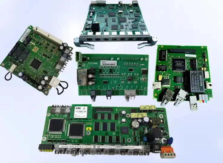
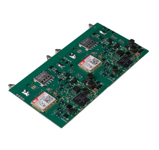
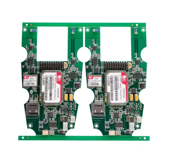
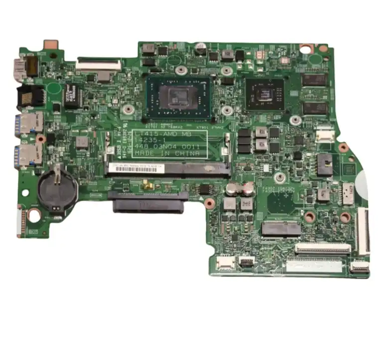
Communication PCBAs (Printed Circuit Board Assemblies) are the backbone of modern telecommunications devices. Designing these intricate boards requires a deep understanding of electrical engineering principles and industry standards. Essential guidelines for Communication PCBA design include optimizing signal integrity, minimizing electromagnetic interference, implementing proper thermal management, and ensuring compliance with regulatory standards. By adhering to these guidelines, engineers can create robust, efficient, and reliable Communication PCBAs that meet the demanding requirements of today's interconnected world.
Optimizing Signal Integrity in Communication PCBAs
Signal integrity is paramount in Communication PCBA design. High-speed digital signals are susceptible to distortion, noise, and crosstalk, which can significantly impact the performance of communication devices. To optimize signal integrity, designers must consider several key factors:

Impedance Matching and Controlled Impedance Routing
Impedance matching is crucial for maintaining signal quality in Communication PCBAs. By ensuring that the impedance of transmission lines matches the source and load impedances, designers can minimize signal reflections and maximize power transfer. Controlled impedance routing involves carefully calculating and maintaining consistent impedance along signal traces. This is typically achieved through precise control of trace width, dielectric thickness, and material properties.
Proper Layer Stack-up Design
The layer stack-up of a Communication PCBA plays a vital role in signal integrity. A well-designed stack-up helps reduce electromagnetic interference (EMI) and improves signal quality. For high-speed designs, it's common to use multiple ground and power planes to provide a low-impedance return path for signals. Alternating signal and ground layers can also help minimize crosstalk between adjacent traces.
Minimizing Crosstalk and EMI
Crosstalk and EMI can severely degrade the performance of Communication PCBAs. To mitigate these issues, designers should implement proper trace routing techniques, such as maintaining adequate spacing between signal traces and using guard traces or ground planes to isolate critical signals. Additionally, employing differential signaling for high-speed communication lines can help reduce EMI and improve noise immunity.
Thermal Management Strategies for Communication PCBAs
Effective thermal management is essential for ensuring the reliability and longevity of Communication PCBAs. As these boards often operate in demanding environments and handle high-frequency signals, they can generate significant heat. Implementing proper thermal management strategies is crucial to prevent component failure and maintain optimal performance.
Heat Dissipation Techniques
Various heat dissipation techniques can be employed in Communication PCBA design. These include the use of thermal vias to conduct heat away from critical components, incorporating copper pours or planes to spread heat across the board, and utilizing heat sinks or cooling fans for active thermal management. The choice of thermal management approach depends on the specific requirements of the design and the operating environment.
Component Placement and Thermal Considerations
Strategic component placement is crucial for effective thermal management. High-power components should be placed in areas with good airflow and away from heat-sensitive elements. Designers should also consider the thermal properties of different PCB materials and choose those with higher thermal conductivity for improved heat dissipation.
Thermal Simulation and Analysis
Advanced thermal simulation tools can help designers predict and optimize the thermal performance of Communication PCBAs. These tools allow engineers to identify potential hotspots, evaluate different cooling strategies, and ensure that all components operate within their specified temperature ranges. Thermal analysis is particularly important for high-density designs and those operating in extreme environments.
Regulatory Compliance and Testing for Communication PCBAs
Communication PCBAs must comply with various regulatory standards and undergo rigorous testing to ensure their performance, reliability, and safety. Adhering to these standards is crucial for market acceptance and legal compliance.
EMC and EMI Standards
Electromagnetic Compatibility (EMC) and Electromagnetic Interference (EMI) standards are critical for Communication PCBAs. These standards, such as FCC Part 15 in the United States or CISPR 22 in Europe, ensure that electronic devices do not interfere with other equipment or communication systems. Designers must implement EMC/EMI mitigation techniques, such as proper shielding, filtering, and grounding, to meet these stringent requirements.
Safety and Environmental Regulations
Communication PCBAs must also comply with safety and environmental regulations. This includes adherence to RoHS (Restriction of Hazardous Substances) directives, which limit the use of certain hazardous materials in electronic equipment. Additionally, safety standards such as UL 60950 for information technology equipment must be met to ensure the product's safe operation.
Performance Testing and Validation
Comprehensive testing and validation are essential to ensure that Communication PCBAs meet their performance specifications. This includes functional testing, environmental stress screening, reliability testing, and signal integrity measurements. Advanced test equipment, such as vector network analyzers and high-speed oscilloscopes, is often used to characterize the performance of high-frequency communication circuits.
Implementing these essential design guidelines for Communication PCBAs is crucial for creating high-performance, reliable, and compliant products. By focusing on signal integrity, thermal management, and regulatory compliance, engineers can develop Communication PCBAs that meet the ever-increasing demands of modern telecommunications devices.
Conclusion
The design of Communication PCBAs is a complex and multifaceted process that requires expertise in various areas of electrical engineering. By following these essential guidelines, designers can create robust and efficient boards that meet the stringent requirements of the telecommunications industry. As technology continues to evolve, staying updated with the latest design techniques and industry standards is crucial for success in this dynamic field.
One-Stop Communication PCBA Assembly & Testing Services
Ring PCB Technology Co., Limited, your trusted PCB Manufacturing Partner since 2008, offers comprehensive one-stop services for Communication PCBA assembly and testing. Our advanced engineering capabilities include high-density stack-up designs with 2-48 layer boards, featuring blind/buried vias and tight 3/3mil trace/spacing. We maintain ±7% impedance control, ideal for 5G, industrial control, medical devices, and automotive electronics.
Our smart manufacturing facility is equipped with state-of-the-art technology, including LDI laser exposure, vacuum lamination, and flying probe testers, adhering to IPC-6012 Class 3 standards. With 17 years of expertise, we deliver innovative, reliable, and cost-effective PCBA solutions tailored to diverse industry needs. Contact us at [email protected] for your Communication PCBA requirements.
References
1. Johnson, H. W., & Graham, M. (2003). High-speed digital design: a handbook of black magic. Prentice Hall PTR.
2. Bogatin, E. (2018). Signal and power integrity–simplified. Prentice Hall Press.
3. Montrose, M. I. (2004). EMC and the printed circuit board: design, theory, and layout made simple. John Wiley & Sons.
4. Coombs, C. F., & Holden, H. T. (2016). Printed circuits handbook. McGraw-Hill Education.
5. Hall, S. H., & Heck, H. L. (2009). Advanced signal integrity for high-speed digital designs. John Wiley & Sons.

Welcome to Ring PCB! Share your inquiry, and receive a tailored quotation!

Ring PCB, your trusted partner for PCB & PCBA Full Turnkey Solutions


