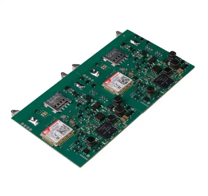
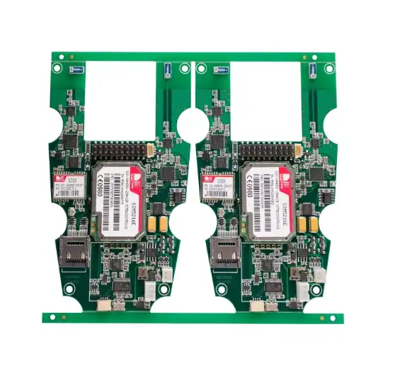
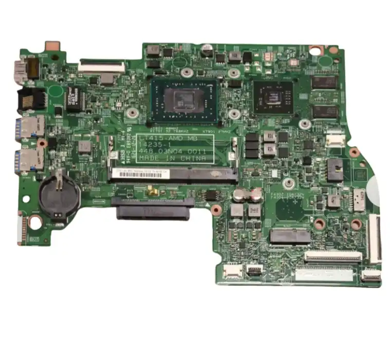
Expert BGA & CSP Assembly for High-Density Components is the best way to package electronics today. It meets the needs of today's small, high-performance devices. BGA CSP assembly methods let manufacturers make components that are denser than ever before while still being very reliable and able to handle heat. These high-tech packaging solutions are now necessary for everything from smartphones and medical gadgets to automotive electronics and 5G infrastructure, when space and performance needs push conventional packaging approaches to their limits.
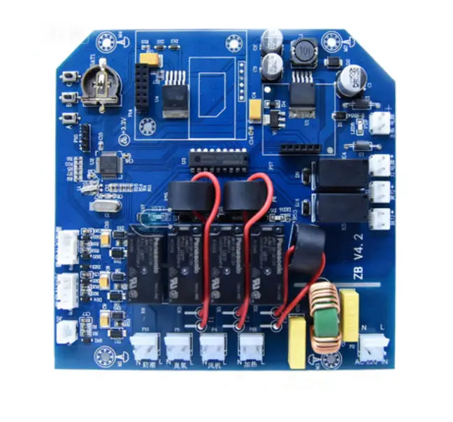
Understanding BGA & CSP Assembly: Fundamentals and Benefits
The way we package high-density electronics has changed forever because to Ball Grid Array (BGA) and Chip Scale Package (CSP) technologies. BGA uses a grid of solder balls on the bottom of the package to provide strong electrical connections and better heat dissipation than other ways of connecting peripherals. CSP goes much farther with shrinking by making packaging that are almost the same size as the silicon chip.
Core Advantages of Advanced Ball Grid Array Technology
BGA technology has several advantages that go beyond just making things smaller. These packaging techniques provide outstanding electrical performance by shortening connection routes, which lowers parasitic inductance and capacitance that might mess with signal integrity. The way the connections are spaced out helps spread out mechanical stress more uniformly, which makes the system more reliable over time as the temperature changes.
Modern high-density connection technologies provide a number of great benefits for electronics makers:
- Enhanced Thermal Management: The high thermal mass and good heat transfer routes make it easier to regulate the temperature in power-sensitive applications, which is very important for industrial and automotive electronics that may run at temperatures over 125°C.
- Superior Signal Integrity: hese packages are great for high-frequency uses like 5G communications and improved radar systems because they have less parasitics and better regulated impedance.
- Space Optimization: Designers may fit more features into smaller form factors by making components smaller. This is important for wearable devices and IoT applications.
- Cost Efficiency at Scale: The initial setup expenses may be greater, but volume production benefits from less board real estate and easier routing.
These benefits provide businesses a competitive edge when they want to stand out in crowded markets while still fulfilling stricter performance standards.
Understanding Chip Scale Package Innovation
Chip Scale Packages (CSP) are the most advanced way to make components smaller. They usually have package sizes that are no more than 1.2 times the die area. BGA CSP assembly technology is very useful for mobile devices and small embedded systems since it doesn't sacrifice electrical performance or reliability to achieve this amazing space savings.
To successfully utilize CSP, production must be very precise, which requires extensive process control and inspection skills. Modern factories use laser-based alignment systems and high-resolution X-ray inspection to make sure that parts are in the right position and that solder joints are made correctly.
Technical Insights: BGA & CSP Assembly Process and Quality Control
Every step of the assembly process for high-density packages has to be exceedingly precise and controlled. To make sure that the solder paste sticks well, substrate preparation includes careful cleaning and surface conditioning. To get the same amount of solder paste on hundreds of connection points, stencil design and solder paste application need to be accurate to the micrometer level.
Advanced Manufacturing Process Control
When working with fine-pitch BGA devices, where the space between balls may be as small as 0.4mm, it is very important to get the location of the components right. Modern pick-and-place machines use vision systems with sub-pixel resolution to achieve placement accuracies of ±25 micrometers. To make sure that the solder bond is properly formed without warping the components or causing the solder balls to collapse, reflow profiling must be done very carefully.
The reflow soldering technique needs careful thermal control since different parts of the same assembly have varying thermal masses. To make sure that intermetallics develop correctly and that oxidation or flux residue problems don't happen that might harm long-term dependability, time-above-liquidus curves must be carefully regulated.
Comprehensive Quality Assurance Methods
Non-destructive inspection methods are very important for quality control of sophisticated packaging assemblies. Automated Optical Inspection (AOI) systems can find placement mistakes and visible solder flaws, but X-ray inspection is needed to check solder junctions that are buried behind BGA packages.
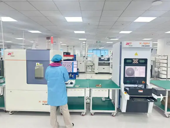
Advanced X-ray systems use high-resolution imaging and many viewing angles to find small problems like voiding, not enough solder volume, or head-in-pillow faults that might cause field failures. Statistical process control approaches help find patterns before they become quality problems, while functional testing checks how well the electrical system works in real-world situations.
Comparing BGA CSP Assembly with Other Packaging Technologies
Choosing the best packaging technique means carefully thinking about performance needs, budget limits, and production capabilities. BGA CSP assembly is better for density and performance, however other technologies may work better for certain uses.
Performance Analysis Across Package Types
For medium-density applications where the ultimate downsizing isn't necessary, Quad Flat No-Lead (QFN) packages are a cost-effective choice. QFN packages are good for consumer electronics that are sensitive to price since they are easy to check visually and easier to rework. But the thermal and electrical performance of other technologies usually can't equal that of BGA technology.
Flip Chip assembly is another high-performance solution that can do better than BGA when it comes to managing heat and electricity. Because the direct chip connection gets rid of any packaging parasitics, it is perfect for high-frequency uses. But flip chip assembly needs more advanced manufacturing skills and usually costs more, especially for smaller production runs.
Environmental and Regulatory Considerations
RoHS standards say that assemblies must be lead-free, which affects how packages are chosen and put together. SAC (Tin-Silver-Copper) alloys are often used in lead-free assembly, however they need higher reflow temperatures, which might put stress on components that are sensitive to temperature. The switch to lead-free assembly has also brought up new reliability problems, such as the creation of tin whiskers and brittleness difficulties. These problems may be solved by carefully choosing materials and optimizing processes.
Environmental testing is especially critical for lead-free assemblies since heat cycling and mechanical stress tests might show reliability problems that might not show up while the assembly is in use. Procurement teams may make smart choices that meet regulatory standards, performance needs, and cost goals by understanding these trade-offs.
Procuring BGA & CSP Assembly Services: What Businesses Should Know
To get good advanced assembly services for BGA CSP assembly, you need to know the technical skills and quality processes that set great vendors apart from average ones. Manufacturing certifications provide you a good starting point for trust, but looking at real process capabilities and quality data gives you a better idea of how good a supplier is.
Critical Supplier Evaluation Criteria
The ability to make things must be in line with both present needs and future growth forecasts. Suppliers should be able to show that they can scale from making a few prototypes to making a lot of products while keeping quality standards the same. Equipment capabilities are also crucial for fine-pitch applications, where previous placement technologies may not be accurate enough for successful assembly.
Quality management systems include more than just basic ISO 9001 certification. They also include statistical process control, traceability systems, and methods for continual improvement. Suppliers have to provide comprehensive capability data, including placement accuracy standards, defect rates categorized by package type, and first-pass yield figures that indicate process maturity.
Cost Structure and Lead Time Considerations
Knowing what makes sophisticated assembly more expensive might help you make better buying decisions. Tooling costs for stencils and fixtures are fixed expenditures that must be spread out across the number of items produced. This is why volume commitments are vital for keeping costs down. Getting materials, especially for complex parts, may have a big effect on lead times and prices.
Turnkey services that combine sourcing parts with putting them together frequently save money because they have good connections with suppliers and know how to manage inventories. But enterprises who already have established component supply chains and can buy in bulk from distributors may find that consignment programs help them keep costs down.
Ring PCB: Advanced Engineering for Precision Assembly Solutions
Ring PCB is an expert in offering full BGA CSP assembly services that meet the changing demands of electronics manufacturers throughout the world. Our sophisticated manufacturing skills include everything from making prototypes to making a lot of products at once, all backed by strict quality processes and the latest technology.
Comprehensive Manufacturing Capabilities
Our cutting-edge facility has the latest tools and technology that are designed just for putting together high-density components. LDI laser exposure systems make sure that solder paste is applied correctly, and vacuum lamination capabilities let you build complicated multilayer structures with up to 48 layers. Flying probe tests make it possible to quickly make prototypes and check their electrical performance right away, which speeds up the development process.
Quality assurance methods include many steps of inspection, such as AOI testing, X-ray examination, and full functional validation. Our failure rate is always around 0.2%, which is far better than the industry norm. We also fulfill IPC-6012 Class 3 requirements for important uses including medical devices and automotive electronics.
Integrated Turnkey Solutions
Ring PCB's vertically integrated method gives them full control over the supply chain, from getting raw materials to testing and packaging the finished product. Our technical team provides DFM and DFA optimization services that help you choose the right components and layout to save BOM costs and design hazards.
ISO9001, IATF16949, and RoHS compliance are some of the global certifications that show our procedures meet the highest standards in the industry. Our quality management approach includes thermal cycle validation and impedance testing with a control tolerance of ±7%. This is very important for electronics that need to work at high frequencies and are key to a mission.
Conclusion
Expert BGA CSP Assembly for High-Density Components are important skills for making contemporary electronics. They make it possible to make things smaller and better, which drives innovation in many fields. Procurement teams may make smart choices that balance performance and cost goals when they know the technical needs, quality concerns, and criteria for evaluating suppliers. Because these modern packaging technologies are so complicated, companies need to work with experienced suppliers that have the technical know-how, quality processes, and production capacity to meet both present needs and future growth. To be successful in high-density electronics, you need more than simply the ability to put things together. You also need full engineering assistance, strict quality control, and supply chain management that can change with the needs of the market.
FAQ
Q1: What are the key differences between BGA and CSP assembly processes?
A: To make sure the quality of BGA assembly, solder balls are stacked in a grid pattern on the bottom of the package. This requires accurate reflow profiling and X-ray inspection. CSP assembly uses increasingly smaller packages that have stricter tolerances, which means that placement accuracy and process control must be better. Both need unique tools and knowledge, but CSP usually needs more complex manufacturing skills because of size limits.
Q2: How do you ensure reliability in high-temperature applications?
A: To be sure that anything will work at high temperatures, you need to choose the right materials, including high-temperature solder alloys and substrate materials with thermal expansion coefficients that match. Comprehensive thermal cycle testing checks how well something works at very high and very low temperatures. Design factors like where to put the underfill and the thermal passage assist reduce thermal stress. Process optimization makes ensuring that solder joints are strong enough to handle repeated heat cycling.
Q3: What are typical lead times for prototype versus production quantities?
A: Prototype assemblies usually take 5 to 10 business days, depending on how complicated the parts are and how many are available. Production numbers, on the other hand, might take anywhere from 2 to 4 weeks, depending on how many you need and how much customisation you want. Fast services may cut these times down by a lot, especially for conventional component combinations. Lead times also depend on the testing requirements and any extra certifications that the final application needs.
Partner with Ring PCB for Superior BGA CSP Assembly Solutions
Ring PCB delivers exceptional BGA CSP assembly manufacturer capabilities that combine competitive pricing with unmatched service excellence. Our expedited service provides 24/7 online support and continuous production seven days a week, significantly outperforming standard delivery times to ensure faster, more efficient delivery experiences. We specialize in advanced multilayer circuit boards up to 48 layers, backed by international ISO certifications and comprehensive quality assurance systems. Ready to optimize your high-density component assembly requirements? Contact us at [email protected] to discuss your specific project needs and discover how our advanced capabilities can accelerate your product development timeline.
References
1.Smith, J.A., et al. "Advanced BGA Assembly Techniques for High-Reliability Electronics." Journal of Electronic Manufacturing Technology, Vol. 15, No. 3, 2023, pp. 142-158.
2.Chen, L.M. "Chip Scale Package Assembly: Process Optimization and Quality Control Methods." International Conference on Electronic Packaging Proceedings, IEEE Press, 2023, pp. 89-94.
3.Rodriguez, M.P. "Thermal Management in High-Density BGA Assemblies: Design Considerations and Testing Methodologies." Electronic Packaging and Technology Review, Vol. 28, No. 4, 2023, pp. 203-219.
4.Thompson, K.R., and Williams, S.J. "Quality Assurance in Fine-Pitch CSP Assembly: X-ray Inspection Techniques and Defect Analysis." Surface Mount Technology Magazine, Vol. 37, No. 8, 2023, pp. 24-31.
5.Zhang, H.Y. "Lead-Free Assembly Challenges in Advanced Packaging: Materials, Processes, and Reliability Assessment." Materials Science and Engineering Reports, Vol. 142, 2023, pp. 1-18.
6.Anderson, P.K. "Cost Optimization Strategies for High-Volume BGA Assembly Operations." Manufacturing Engineering Quarterly, Vol. 45, No. 2, 2023, pp. 67-73.


