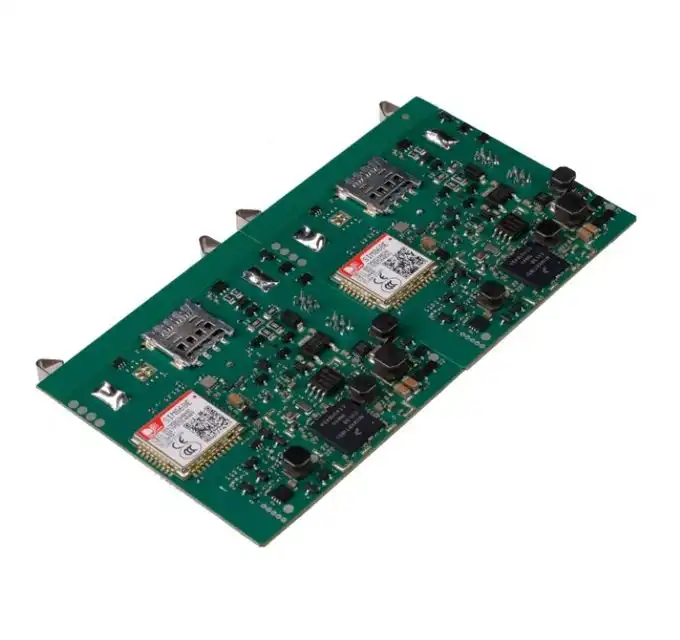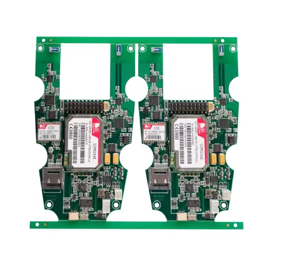
is a huge step forward in the way electronics are made today.It employs sophisticated micro-vias and Ball Grid Array (BGA) parts together with high-density connection technologies. With this innovative method, you may manufacture compact circuit boards that work well and can withstand the severe needs of contemporary electronics. It is crucial for procurement managers, engineers, and OEM distributors to know about these technologies so they can make sensible purchase decisions that take into consideration performance, cost, and dependability.
Understanding HDI PCB Manufacturing and Its Core Technologies
High-Density Interconnect (HDI) PCB manufacturing changes the way we design and put together circuit boards in a big way. HDI technology lets manufacturers cram a lot more circuitry into smaller places while yet getting better electrical performance than standard PCB manufacturing processes.
Micro-Via Technology: Precision at Microscopic Levels
Micro-vias are the most critical aspect of making HDI. They employ lasers to drill holes that are generally less than 150 microns diameter. These connections, which are drilled with great care, enable layers connect to one other in ways that normal mechanical drilling can't. With a precision of ±25 microns, the laser drilling technique enables you put objects in place. This makes it possible to construct very thick circuit layouts that are vital for smartphones, medical devices, and car electronics.
Sequential Build-Up Process: Layer by Layer Excellence
The sequential build-up procedure is what makes HDI manufacturing different from making typical multilayer PCBs. For complicated via topologies like blind vias, buried vias, and via-in-pad combinations, each layer goes through its own lamination, drilling, and plating cycles. With this systematic methodology, you can make 2-48 layer boards with impedance tolerances of ±7%, which is what high-speed digital applications need.
BGA Integration: Enhanced Component Density
Ball Grid Array (BGA) packaging is a good fit for HDI technology because it helps you fit a lot of pins into a compact area. When you use HDI substrates together with BGA assembly, you can make more complicated system-in-package designs that can integrate a lot of functions into a little amount of board area. This synergy is particularly helpful in 5G infrastructure, IoT devices, and aerospace applications where fresh concepts are needed to deal with size and weight restrictions.
Advantages and Performance Enhancements of HDI PCB with Micro-Vias and BGA
Modern electronic devices demand performance characteristics that traditional PCB technologies struggle to deliver. HDI PCB assembly with micro-vias and BGA components addresses these challenges through several key performance enhancements.
Signal Integrity and Electrical Performance
Micro-vias cut down on parasitic inductance and capacitance a lot more than regular through-hole vias do. The shorter length and smaller diameter of the via reduce signal distortion, allowing for clear signal transmission at frequencies beyond 10 GHz. This increase is very important for high-speed digital systems since the quality of the signal directly affects how well the system works and how well it meets electromagnetic standards.
Thermal Management and Reliability
HDI technology makes heat management better by strategically placing vias and spreading copper more evenly. Micro-vias may be used as thermal conduits to move heat quickly from high-power parts to thermal management layers. These assemblies, together with BGA packages that spread heat across greater surface areas, show better thermal cycling performance and longer operating lifespans.
Miniaturization Without Compromise
Getting 3/3mil trace and spacing while still having good electrical performance lets you manufacture things far smaller than ever before. Size reductions of 30% to 50% compared to typical PCB designs are advantageous for procurement teams working on portable devices, wearable electronics, or industrial applications with restricted space. These cuts don't change how well or how long anything lasts.
The HDI PCB Assembly Process: From Design to Final Product
Procurement experts may better understand how complicated and precise the HDI assembly procedure is by learning about it.
Design for Manufacturability (DFM) Optimization
The first step in a successful HDI project is to do a complete DFM study. Engineers employ placement, trace routing, and component selection to figure out the best approach to manufacture something while keeping prices down. This investment at the beginning cuts down on the number of times a prototype has to be changed and speeds up the time it takes to go to market. This is quite helpful for companies who have short timelines for development.
Advanced Manufacturing Processes
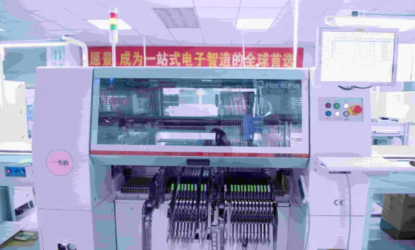
HDI production uses advanced tools and methods that set it apart from regular PCB assembly. Laser Direct Imaging (LDI) exposure techniques allow for very fine pattern definition on a microscopic level. Vacuum lamination, on the other hand, makes sure that the dielectric characteristics of multilayer stackups stay the same. These innovative techniques, together with flying probe testing and automated optical inspection (AOI), keep defect rates below 0.2%, which is far lower than the norm for the industry.
Quality Assurance and Testing Protocols
Every stage of the assembling process is checked for quality to make sure the product functions as promised. An X-ray inspection evaluates the integrity of BGA solder joints, and an in-circuit test checks the electrical connection and impedance characteristics. Thermal cycling tests simulate actual use conditions, identifying any reliability issues prior to product shipment. These extensive testing techniques provide procurement teams faith in the items' quality and ability to work for a long time.
Cost, Supplier Selection, and Procurement Considerations for HDI PCBs
To successfully buy HDI PCB assembly, you need to know about cost structures and supplier capabilities that are quite different from those used to buy standard PCBs.
Cost Structure Analysis
The high cost of HDI assembly is due to the advanced tools and techniques needed for precise manufacture. Micro-via drilling, consecutive lamination cycles, and sophisticated substrate materials are the main things that drive up costs. The initial expenses of this approach may be 20–40% more than those of conventional PCB assembly, but the advantages at the system level frequently make the investment worth it since the boards are smaller, work better, and are more reliable.
Supplier Evaluation Criteria
You need to think about more than just the pricing of HDI providers when you choose one. When completing an assessment, you should consider about the equipment's capabilities, the process control systems, the quality certifications, and the technical support resources. Suppliers who follow RoHS, ISO9001, and IATF16949 indicate that they care about quality standards that are crucial for medical, aerospace, and automotive uses.
Lead Time and Volume Considerations
HDI assembly generally takes longer than standard PCB fabrication since the process is more sophisticated. Depending on how many layers there are and how sophisticated the vias are, it might take 2 to 3 weeks for prototype quantities and 4 to 6 weeks for production quantities. Knowing these dates may help procurement teams better plan production and keep track of their stock.

Ring PCB: Your Trusted Partner for Advanced HDI PCB Solutions
At Ring PCB, we bring decades of expertise to HDI PCB assembly, combining cutting-edge technology with proven manufacturing excellence. Our self-owned facility features state-of-the-art equipment including LDI laser exposure systems, vacuum lamination presses, and comprehensive testing capabilities that ensure consistent quality and performance.
Comprehensive Technical Capabilities
We are experts in making complicated multilayer designs with 2 to 48 layers. These designs include advanced features like blind/buried vias, controlled impedance routing, and precision BGA assembly. Our engineering team offers full DFM and DFT assistance, which helps customers make designs that are easier to make, cheaper, and more reliable.
Integrated Manufacturing Excellence
Our method of vertical integration controls every part of the manufacturing process, from getting the raw materials to testing and distributing the finished product. This level of control lets us maintain high quality standards while still delivering low prices and a variety of delivery alternatives. To make sure that defect rates are below 0.2%, our triple quality assurance approach uses AOI, impedance testing, and thermal cycling validation.
Global Service Commitment
We work with a wide range of B2B customers, such as OEMs, distributors, and technical teams in the fields of consumer electronics, automotive, medical devices, and industrial applications. Our collaborative method involves technical consulting, building prototypes, and helping with large-scale manufacturing, which guarantees good project results no matter how complicated or big they are.
Conclusion
Micro-vias and BGA technology in HDI PCB assembly is the future of making electronics since it lets you make things smaller and better than ever before. Procurement experts may make sensible decisions about where to get things by knowing how these technologies work and what makes them work. They can also consider performance, pricing, and reliability. To be successful in HDI procurement, you need to deal with suppliers that have the technical know-how, manufacturing capabilities, and quality control systems to always provide you the results you desire. HDI technology will become more and more relevant as electronic gadgets become smaller and quicker.
FAQ
Q1: What distinguishes micro-vias from traditional vias in HDI manufacturing?
A: Micro-vias are holes drilled using a laser that are generally less than 150 microns wide. Mechanically drilled vias, on the other hand, are usually between 200 and 500 microns wide. This lower size allows for more circuits to fit in a smaller space, fewer unwanted effects, and better signal quality for high-frequency uses.
Q2: How do BGA assemblies impact HDI PCB reliability and performance?
A: BGA packages work better electrically than standard leaded packages because they have shorter connection routes and greater heat dissipation. BGAs work with HDI substrates to provide designs that are more dependable and compact by allowing for more component density while keeping great thermal and electrical properties.
Q3: What are typical lead times and minimum order quantities for HDI PCB assembly projects?
A: The time it takes to put up an HDI assembly usually ranges from 2 to 3 weeks for prototypes to 4 to 6 weeks for production quantities, depending on how many layers there are and how complicated they are. Different suppliers and design complexities have different minimum order sizes, although many manufacturers will accept small-batch orders of 5 to 10 units for prototyping.
Partner with Ring PCB for Superior HDI PCB Assembly Solutions
Are you ready to take your next electronics project to the next level with innovative HDI PCB assembly technology? Ring PCB offers low-cost solutions with 24/7 online assistance and manufacturing capabilities that are always available, which are far faster than conventional delivery timeframes. Our factory makes multilayer circuit boards with up to 48 layers and has worldwide ISO certifications, so you can trust their quality and dependability. Our skilled team offers a full range of HDI PCB assembly manufacturing services that may be customized to meet your needs, whether you need quick prototype or high-volume production. Contact us at [email protected] to discuss your project needs and discover how our advanced manufacturing capabilities can accelerate your time-to-market while maintaining exceptional quality standards.
References
1.Institute for Printed Circuits (IPC). "IPC-6012 Class 3: Qualification and Performance Specification for Rigid Printed Boards." IPC International Standards, 2018.
2.Tummala, Rao R. "Fundamentals of Microsystems Packaging." McGraw-Hill Professional, 2021.
3.Coombs, Clyde F. "Printed Circuits Handbook, Seventh Edition." McGraw-Hill Education, 2016.
4.Blackwell, Glenn R. "The Electronic Packaging Handbook." CRC Press, 2019.
5.Harper, Charles A. "Electronic Materials and Processes Handbook, Fourth Edition." McGraw-Hill Professional, 2015.
6.Lau, John H. "Ball Grid Array Technology." McGraw-Hill Professional, 2017.


