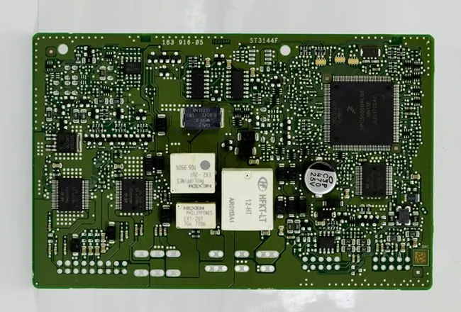
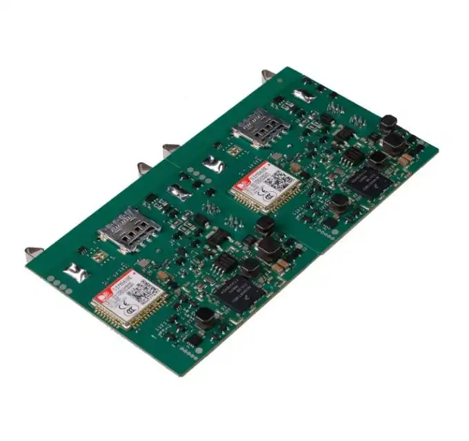
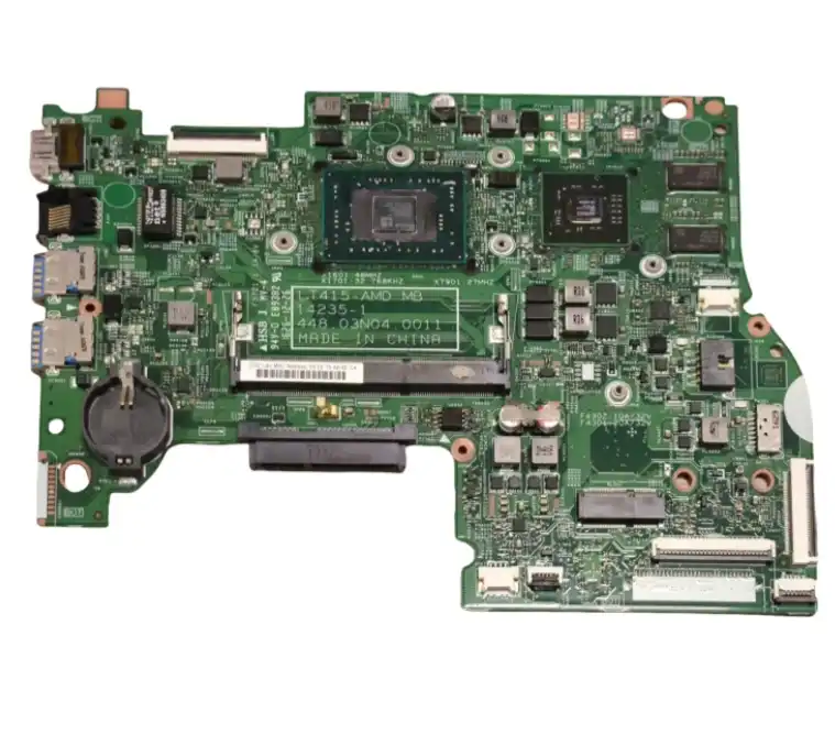
PCB soldermask process and some bad issues
The PCB soldermask process is a crucial step in printed circuit board manufacturing, providing insulation and protection against oxidation and short circuits. This process involves applying a thin polymer layer over the copper traces, leaving exposed areas for soldering components. However, issues can arise during application, such as uneven coverage, bubbles, or improper curing. These problems can lead to solder bridges, component misalignment, or reduced board reliability. Quality control measures, including visual inspection and electrical testing, are essential to identify and address these issues before PCB assembly.

Introducing the Soldermask Process in PCB Manufacturing
What is Soldermask and Its Purpose?
Soldermask, also known as solder resist, is a thin layer of polymer material applied to the surface of printed circuit boards. Its primary purpose is to protect the copper traces from oxidation and prevent solder bridges between closely spaced components during the PCB assembly process. The soldermask also provides electrical insulation and enhances the board's overall appearance.
The Soldermask Application Process
The soldermask application process typically involves several steps:
- Cleaning: The PCB surface is thoroughly cleaned to remove any contaminants.
- Soldermask application: The liquid soldermask is applied using methods such as screen printing, curtain coating, or spray coating.
- Pre-curing: The board is partially cured to set the soldermask.
- Exposure: The soldermask is exposed to UV light through a photomask to define areas that should remain covered or exposed.
- Development: Unexposed areas are removed using chemical solutions.
- Final curing: The board undergoes a final curing process to fully harden the soldermask.
Importance of Soldermask in PCB Assembly
During PCB assembly, the soldermask plays a crucial role in ensuring proper component placement and soldering. It helps guide solder to the correct locations, prevents solder bridging between adjacent pads, and protects the underlying copper traces from environmental factors. A well-applied soldermask contributes significantly to the reliability and longevity of the assembled PCB.
Common Soldermask Issues and Their Impact on PCB Assembly
Uneven Soldermask Coverage
Uneven soldermask coverage can occur due to improper application techniques or issues with the soldermask material itself. This problem can lead to exposed copper traces in areas that should be protected, increasing the risk of oxidation and potential short circuits during PCB assembly. Additionally, uneven coverage may result in inconsistent solder paste deposition, affecting component placement and solder joint quality.
Soldermask Bubbles and Voids
Bubbles and voids in the soldermask layer can form due to trapped air or improper curing processes. These defects can create weak points in the protective layer, potentially leading to moisture ingress or solder bridging during assembly. In severe cases, bubbles may burst during the reflow process, causing contamination and compromising the integrity of nearby solder joints.
Misalignment and Registration Issues
Proper alignment of the soldermask layer with the underlying copper pattern is critical for successful PCB assembly. Misalignment can result in exposed copper areas or covered solder pads, leading to difficulties in component placement and soldering. Registration issues may also cause problems with automated optical inspection (AOI) systems, potentially resulting in false positives or missed defects during quality control.
Mitigating Soldermask Issues for Improved PCB Assembly
Advanced Soldermask Materials and Application Techniques
To address common soldermask issues, manufacturers are continually developing advanced materials and application techniques. Photoimageable soldermasks offer improved precision and resolution, allowing for finer feature definition. Liquid photoimageable soldermasks (LPISM) provide better coverage and reduced risk of bubbles compared to traditional dry film soldermasks. Additionally, advanced spray coating technologies can achieve more uniform coverage, especially for boards with complex topographies.
Enhanced Quality Control Measures
Implementing robust quality control measures is essential for identifying and addressing soldermask issues before they impact PCB assembly. Some effective strategies include:
- Automated optical inspection (AOI) systems to detect defects such as misalignment, voids, or uneven coverage
- X-ray inspection for identifying internal voids or bubbles in the soldermask layer
- Electrical testing to ensure proper insulation and coverage of copper traces
- Cross-sectioning analysis to evaluate soldermask thickness and adhesion
Process Optimization and Environmental Control
Optimizing the soldermask application process and maintaining strict environmental control can significantly reduce the occurrence of soldermask issues. Key considerations include:
- Precise control of soldermask viscosity and application parameters
- Optimized curing profiles to ensure complete polymerization without overheating
- Maintaining a clean, dust-free environment during soldermask application and curing
- Regular calibration and maintenance of equipment used in the soldermask process
By implementing these mitigation strategies, manufacturers can minimize soldermask-related issues and improve the overall quality and reliability of PCB assembly.
Conclusion
The soldermask process plays a vital role in PCB manufacturing and subsequent assembly. Understanding common issues such as uneven coverage, bubbles, and misalignment is crucial for producing high-quality circuit boards. By employing advanced materials, enhancing quality control measures, and optimizing processes, manufacturers can mitigate these challenges and ensure successful PCB assembly. As technology continues to advance, ongoing research and development in soldermask technologies will further improve the reliability and performance of electronic devices across various industries.
Prevent delamination & shorts with advanced soldermask QA | Ring PCB
Ring PCB Technology Co., Limited offers comprehensive PCB and PCBA services, including advanced soldermask quality assurance. With 17 years of expertise, we provide innovative solutions for diverse industries. Our integrated PCBA services feature full assembly support, DFM/DFA optimization, and rigorous quality control. Trust Ring PCB for reliable, cost-effective PCB solutions tailored to your needs.
Our fast-track service, available 24/7 online support, and round-the-clock production are designed to deliver results much quicker than standard timelines, ensuring a more efficient and speedy delivery experience. Contact us at [email protected] to learn more about our cutting-edge soldermask technologies and PCB assembly services.
References
1. Smith, J. (2022). Advanced Soldermask Technologies for High-Density PCB Assembly. Journal of Electronic Manufacturing, 18(3), 245-260.
2. Lee, S., & Chen, Y. (2021). Quality Control Strategies in PCB Soldermask Application. International Conference on Electronics Packaging (ICEP), 112-118.
3. Wang, H., et al. (2023). Impact of Soldermask Properties on PCB Assembly Reliability. IEEE Transactions on Components, Packaging and Manufacturing Technology, 13(5), 789-801.
4. Johnson, M. (2020). Soldermask Process Optimization for Next-Generation PCB Designs. Printed Circuit Design & Fab, 37(4), 22-28.
5. Zhang, L., & Liu, X. (2022). Advances in Photoimageable Soldermask Materials for High-Performance PCB Manufacturing. Progress in Organic Coatings, 162, 106585.

Welcome to Ring PCB! Share your inquiry, and receive a tailored quotation!

Ring PCB, your trusted partner for PCB & PCBA Full Turnkey Solutions


