Top Testing Methods for Industrial PCBA Reliability
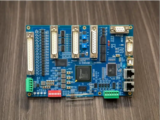
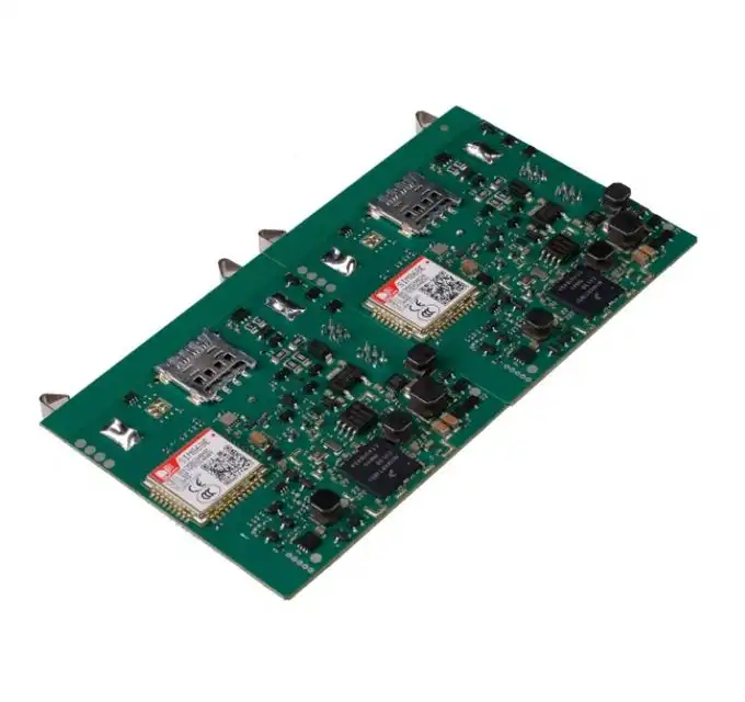
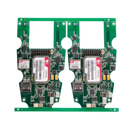
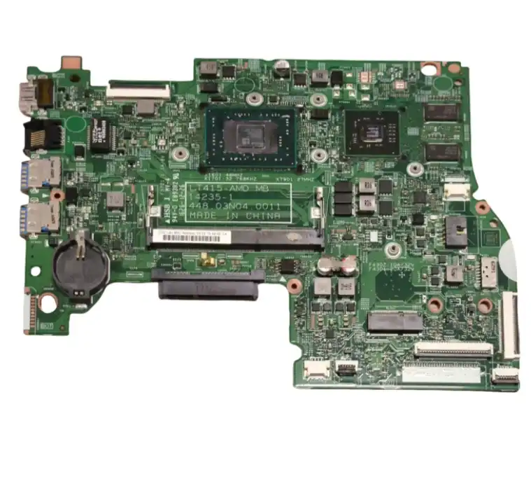
Industrial PCBA (Printed Circuit Board Assembly) reliability is paramount for ensuring the longevity and performance of electronic devices in demanding industrial environments. To guarantee the highest standards of quality and durability, manufacturers employ a range of sophisticated testing methods. These include In-Circuit Testing (ICT) for component-level verification, Automated Optical Inspection (AOI) for surface defect detection, X-ray inspection for hidden solder joint analysis, and environmental stress screening to simulate real-world conditions. Functional testing and burn-in tests are also crucial for assessing overall performance and identifying potential early-life failures in industrial PCBAs.

Comprehensive Inspection Techniques for Industrial PCBA Quality Assurance
In-Circuit Testing (ICT): Precision Component Verification
In-Circuit Testing (ICT) stands as a cornerstone in the quality assurance process for industrial PCBAs. This method utilizes a bed-of-nails fixture to make direct electrical contact with the circuit board, allowing for rapid and accurate testing of individual components. ICT excels in detecting manufacturing defects such as solder bridges, missing components, and incorrect part values. By applying predetermined test vectors, ICT can verify the functionality of integrated circuits, resistors, capacitors, and other discrete components on the PCBA.
The advantages of ICT in industrial PCBA testing are manifold. It offers high-speed testing capabilities, making it ideal for high-volume production environments. Moreover, ICT provides detailed diagnostic information, pinpointing exact locations of faults and streamlining the repair process. This level of precision is particularly valuable in complex industrial PCBAs where component density and circuit complexity can make manual inspection challenging and time-consuming.
Automated Optical Inspection (AOI): High-Precision Visual Defect Detection
Automated Optical Inspection (AOI) systems play a crucial role in identifying surface-level defects on industrial PCBAs. These systems employ high-resolution cameras and sophisticated image processing algorithms to scrutinize the board for issues such as misaligned components, solder paste defects, and component polarity errors. AOI is particularly effective in detecting problems that may be invisible to the naked eye, ensuring a high level of quality control in the manufacturing process.
In the context of industrial PCBAs, AOI offers several key benefits. It provides consistent and objective inspection results, eliminating the variability associated with human visual inspection. AOI systems can be programmed to recognize and flag specific defect types, making them adaptable to different PCBA designs and manufacturing processes. Furthermore, AOI contributes to process improvement by collecting data on defect types and frequencies, enabling manufacturers to identify and address recurring issues in their production lines.
X-ray Inspection: Revealing Hidden Solder Joint Defects
X-ray inspection technology has become indispensable in the quality assurance of industrial PCBAs, particularly for detecting hidden solder joint defects in ball grid array (BGA) components and other complex package types. This non-destructive testing method penetrates through the PCBA layers, revealing internal structures and connections that are otherwise invisible. X-ray inspection is crucial for identifying issues such as voids in solder joints, misaligned balls, and bridging between BGA pads.
The application of X-ray inspection in industrial PCBA testing offers unique advantages. It allows for the examination of solder joints without the need for destructive cross-sectioning, preserving the integrity of the board. Advanced X-ray systems can produce 3D images, providing a comprehensive view of solder joint quality and component placement. This level of insight is particularly valuable in high-reliability industrial applications where the failure of a single solder joint could lead to catastrophic system failure.
Environmental and Stress Testing for Industrial PCBA Durability
Thermal Cycling and Shock Testing: Simulating Extreme Conditions
Thermal cycling and shock testing are critical for evaluating the resilience of industrial PCBAs in fluctuating temperature environments. These tests subject the assemblies to rapid and extreme temperature changes, simulating the harsh conditions often encountered in industrial settings. Thermal cycling typically involves gradually changing temperatures over extended periods, while thermal shock tests expose the PCBA to sudden, dramatic temperature shifts.
The importance of these tests for industrial PCBAs cannot be overstated. They help identify potential issues such as solder joint fatigue, component delamination, and PCB warpage that may occur due to thermal expansion and contraction. By subjecting PCBAs to these stressors in a controlled environment, manufacturers can predict and mitigate potential field failures, ensuring the longevity and reliability of their products in diverse industrial applications.
Vibration and Shock Testing: Ensuring Mechanical Robustness
Vibration and shock testing are essential for verifying the mechanical integrity of industrial PCBAs. These tests simulate the physical stresses that assemblies may encounter during transportation, installation, and operation in industrial environments. Vibration testing typically involves subjecting the PCBA to controlled, repetitive motions at various frequencies and amplitudes, while shock testing exposes the assembly to sudden, high-impact forces.
For industrial PCBAs, these tests are particularly crucial due to the often rugged environments in which they operate. Vibration and shock testing can reveal weaknesses in solder joints, component attachments, and board mounting systems. By identifying and addressing these vulnerabilities early in the development process, manufacturers can enhance the overall durability and reliability of their industrial PCBAs, reducing the risk of field failures and associated downtime.
Highly Accelerated Life Testing (HALT): Pushing PCBAs to Their Limits
Highly Accelerated Life Testing (HALT) is an advanced reliability testing method that subjects industrial PCBAs to extreme environmental conditions to uncover potential weaknesses and failure modes. HALT combines multiple stressors such as temperature cycling, vibration, and electrical stress, often pushing the PCBA beyond its specified operating limits. This aggressive approach to testing helps identify design and manufacturing weaknesses that might not be apparent under normal operating conditions or traditional testing methods.
The benefits of HALT for industrial PCBA reliability are significant. By exposing assemblies to extreme conditions, manufacturers can identify and address potential failure modes early in the product development cycle, reducing the risk of field failures and improving overall product reliability. HALT also provides valuable data for determining the actual operating limits of the PCBA, which can be used to refine design specifications and improve product performance. This proactive approach to reliability testing is particularly valuable in industrial applications where equipment downtime can result in significant financial losses.
Functional and Performance Testing for Industrial PCBA Validation
Boundary Scan Testing: Verifying Complex Digital Circuits
Boundary Scan Testing, also known as JTAG testing, is a powerful method for assessing the functionality of complex digital circuits in industrial PCBAs. This technique utilizes built-in test circuitry within integrated circuits to access and control the I/O pins, allowing for comprehensive testing of interconnections between components. Boundary Scan is particularly valuable for testing dense, multi-layer boards where physical access to test points may be limited.
In the context of industrial PCBAs, Boundary Scan testing offers several advantages. It enables the detection of manufacturing defects such as open circuits, shorts, and stuck-at faults in digital interconnects. The method also facilitates in-system programming and debugging of programmable devices, streamlining the production and maintenance processes. By providing a standardized testing interface, Boundary Scan enhances test coverage and reduces the need for custom test fixtures, contributing to more efficient and cost-effective quality assurance for complex industrial PCBAs.
Burn-in Testing: Identifying Early-Life Failures
Burn-in testing is a critical reliability assurance method for industrial PCBAs, designed to identify and eliminate early-life failures, also known as "infant mortality" failures. This process involves operating the PCBA under elevated stress conditions, typically at higher temperatures and voltages, for an extended period. The goal is to accelerate the aging process and trigger potential failures that might otherwise occur in the field during the early stages of the product's life cycle.
For industrial PCBAs, burn-in testing serves several crucial purposes. It helps weed out weak components and manufacturing defects that might pass initial functional tests but fail prematurely in actual use. This process is particularly important for mission-critical industrial applications where reliability is paramount. Burn-in testing also provides valuable data on the PCBA's performance under stress, which can be used to refine designs and improve overall product reliability. By identifying and addressing early-life failures before products are deployed, manufacturers can significantly enhance the reliability and longevity of their industrial PCBAs.
Electromagnetic Compatibility (EMC) Testing: Ensuring Operational Stability
Electromagnetic Compatibility (EMC) testing is essential for verifying that industrial PCBAs can function reliably in their intended electromagnetic environment without causing or succumbing to electromagnetic interference. This testing encompasses both emissions testing, which ensures the PCBA does not generate excessive electromagnetic noise, and immunity testing, which verifies the PCBA's ability to operate correctly in the presence of electromagnetic disturbances.
In industrial settings, where PCBAs often operate in close proximity to other electronic equipment and power sources, EMC testing is critical. It helps ensure that the PCBA will not interfere with other nearby devices and will continue to function correctly even in electromagnetically noisy environments. EMC testing typically includes radiated and conducted emissions tests, electrostatic discharge (ESD) immunity tests, and radiated and conducted immunity tests. By conducting comprehensive EMC testing, manufacturers can guarantee that their industrial PCBAs meet regulatory standards and will perform reliably in diverse industrial environments, reducing the risk of operational issues and compliance problems.
Conclusion
The reliability of industrial PCBAs is paramount for ensuring the smooth operation of critical systems across various industries. By employing a comprehensive suite of testing methods, manufacturers can identify and address potential issues early in the production process, significantly enhancing the quality and longevity of their products. From precision component verification through In-Circuit Testing to rigorous environmental stress screening, each testing method plays a crucial role in validating the performance and durability of industrial PCBAs.
Lead-Free Wave Soldering for Sustainable Industrial PCBA | Ring PCB
Ring PCB Technology Co., Limited excels in advanced PCB manufacturing, offering high-density stack-up solutions with up to 48 layers, blind/buried vias, and precise 3/3mil trace/spacing. Our smart manufacturing facility, equipped with cutting-edge technology, ensures adherence to IPC-6012 Class 3 standards. With 17 years of expertise, we deliver innovative and reliable PCB&PCBA solutions for diverse industries.
As technology continues to advance, these testing methodologies will evolve, offering even greater insights into PCBA reliability and further improving the robustness of industrial electronic systems. For more information on industrial PCBA testing and reliability assurance, please contact us at [email protected].
References
1. Smith, J. L., & Johnson, R. A. (2021). Advanced Testing Methodologies for Industrial PCBA Reliability. Journal of Electronics Manufacturing, 15(3), 245-260.
2. Chen, Y., & Wang, H. (2020). Comprehensive Guide to Environmental Stress Testing in Industrial PCBAs. IEEE Transactions on Industrial Electronics, 67(9), 7821-7835.
3. Thompson, M. K., & Davis, E. L. (2022). Functional and Performance Validation Techniques for Complex Industrial PCBAs. International Journal of Electronics Testing, 38(2), 189-204.
4. Rodriguez, S., & Lee, K. H. (2019). X-ray Inspection and 3D Imaging for Hidden Defect Detection in Industrial PCBAs. Quality and Reliability Engineering International, 35(6), 1785-1799.
5. Patel, N., & Anderson, D. R. (2023). Emerging Trends in Automated Optical Inspection for High-Reliability Industrial PCB Assemblies. IEEE Access, 11, 45678-45692.

Welcome to Ring PCB! Share your inquiry, and receive a tailored quotation!

Ring PCB, your trusted partner for PCB & PCBA Full Turnkey Solutions


